MT46V32M16P-5B AIT:J TR
| Part Description |
IC DRAM 512MBIT PARALLEL 66TSOP |
|---|---|
| Quantity | 1,282 Available (as of June 14, 2026) |
| Product Category | Memory |
|---|---|
| Manufacturer | Micron Technology Inc. |
| Manufacturing Status | Obsolete |
| Manufacturer Standard Lead Time | Contact Us |
| Datasheet |
Specifications & Environmental
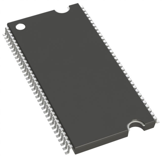
| Device Package | 66-TSOP | Memory Format | DRAM | Technology | SDRAM - DDR | ||
|---|---|---|---|---|---|---|---|
| Memory Size | 512 Mbit | Access Time | 700 ps | Grade | Automotive | ||
| Clock Frequency | 200 MHz | Voltage | 2.5V ~ 2.7V | Memory Type | Volatile | ||
| Operating Temperature | -40°C ~ 85°C (TA) | Write Cycle Time Word Page | 15 ns | Packaging | 66-TSSOP (0.400", 10.16mm Width) | ||
| Mounting Method | Volatile | Memory Interface | Parallel | Memory Organization | 32M x 16 | ||
| Moisture Sensitivity Level | 3 (168 Hours) | RoHS Compliance | ROHS3 Compliant | REACH Compliance | REACH Unaffected | ||
| Qualification | AEC-Q100 | ECCN | EAR99 | HTS Code | 8542.32.0036 |
Overview of MT46V32M16P-5B AIT:J TR – IC DRAM 512MBIT PARALLEL 66TSOP
The MT46V32M16P-5B AIT:J TR is a 512 Mbit DDR SDRAM organized as 32M × 16 with a parallel memory interface in a 66-pin TSSOP package. It implements a double-data-rate, internal pipelined architecture with four internal banks for concurrent operation and source‑synchronous data capture.
Designed for applications that require mid-density, high-speed parallel memory, this device provides a 200 MHz clock rating (DDR), fast access timing, and automotive-grade qualification suitable for demanding temperature environments and reliability requirements.
Key Features
- Core / Architecture Double-data-rate (DDR) SDRAM with an internal, pipelined DDR architecture and four internal banks to enable two data accesses per clock cycle.
- Memory Organization & Capacity 32M × 16 configuration delivering 512 Mbit of volatile DRAM storage with parallel data interface.
- Performance & Timing Rated for a 200 MHz clock frequency (DDR) with an access time of 700 ps and a write cycle time (word page) of 15 ns; programmable burst lengths of 2, 4, or 8.
- Data Integrity & Capture Bidirectional data strobe (DQS) transmitted/received with data for source‑synchronous capture, DLL to align DQ/DQS with the clock, and data mask (DM) for write masking (two DM signals on x16).
- Clock & Command Differential clock inputs (CK, CK#) with commands entered on positive CK edges for synchronous operation.
- Power Operates from a 2.5 V–2.7 V supply range (VDD / VDDQ), with SSTL_2 compatible 2.5 V I/O.
- Package 66‑pin TSSOP (0.400", 10.16 mm width) with longer‑lead TSOP option noted for improved reliability.
- Temperature & Qualification Operating temperature range −40°C to +85°C (TA) and AEC‑Q100 qualification for applications requiring enhanced component reliability.
Typical Applications
- Automotive electronic systems Use as parallel DDR system memory where AEC‑Q100 qualification and −40°C to +85°C operation are required.
- Embedded controllers and processors Provides mid-density volatile storage for buffering and working memory in embedded designs that need a parallel DDR interface.
- Multimedia and display subsystems Acts as frame or data buffer memory in systems that need burst transfers and source‑synchronous data capture.
Unique Advantages
- AEC‑Q100 qualified: Provides a recognized reliability standard suitable for designs that require automotive-grade component qualification.
- DDR performance at 200 MHz: Supports double-data-rate operation and a 200 MHz clock rating for higher effective throughput compared with single‑rate DRAM.
- Source-synchronous capture with DQS and DLL: DQS per byte and DLL alignment enable robust read/write timing and tighter data capture windows.
- Flexible burst and bank operation: Programmable burst lengths (2/4/8) and four internal banks enable efficient block transfers and concurrent memory operations.
- Automotive temperature range: Specified for −40°C to +85°C operation to meet thermal requirements in temperature‑sensitive environments.
- Industry-standard 66‑TSSOP package: Compact footprint with a longer‑lead TSOP option for improved reliability in soldering and mechanical stress conditions.
Why Choose IC DRAM 512MBIT PARALLEL 66TSOP?
The MT46V32M16P-5B AIT:J TR combines DDR architecture, a 32M × 16 organization, and automotive qualification to deliver reliable, mid-density parallel memory for systems that demand verified component robustness and predictable timing. Its 2.5 V I/O, DQS-based source-synchronous capture, and DLL alignment provide deterministic timing characteristics for embedded designs requiring DDR performance.
This device is well suited for designers and OEMs building automotive and industrial systems that need AEC‑Q100 qualified DRAM with a standard 66‑TSSOP package, predictable timing, and flexible burst operation for buffering, frame storage, or working memory duties.
Request a quote or submit an inquiry for availability, pricing, and lead-time information for the MT46V32M16P-5B AIT:J TR.