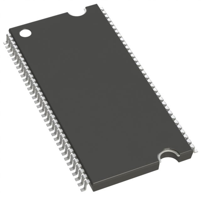
MT46V32M16P-5B L:J
| Part Description |
IC DRAM 512MBIT PARALLEL 66TSOP |
|---|---|
| Quantity | 1,197 Available (as of June 15, 2026) |

| Product Category | Memory |
|---|---|
| Manufacturer | Micron Technology Inc. |
| Manufacturing Status | Obsolete |
| Manufacturer Standard Lead Time | Contact Us |
| Datasheet |
Specifications & Environmental
| Device Package | 66-TSOP | Memory Format | DRAM | Technology | SDRAM - DDR | ||
|---|---|---|---|---|---|---|---|
| Memory Size | 512 Mbit | Access Time | 700 ps | Grade | Commercial | ||
| Clock Frequency | 200 MHz | Voltage | 2.5V ~ 2.7V | Memory Type | Volatile | ||
| Operating Temperature | 0°C ~ 70°C (TA) | Write Cycle Time Word Page | 15 ns | Packaging | 66-TSSOP (0.400", 10.16mm Width) | ||
| Mounting Method | Volatile | Memory Interface | Parallel | Memory Organization | 32M x 16 | ||
| Moisture Sensitivity Level | 3 (168 Hours) | RoHS Compliance | ROHS Compliant | REACH Compliance | REACH Unaffected | ||
| Qualification | N/A | ECCN | EAR99 | HTS Code | 8542.32.0036 |
Overview of MT46V32M16P-5B L:J – IC DRAM 512MBIT PARALLEL 66TSOP
The MT46V32M16P-5B L:J is a 512 Mbit Double Data Rate (DDR) SDRAM organized as 32M × 16 with a parallel memory interface in a 66‑TSSOP package. It implements an internal, pipelined DDR architecture that performs two data accesses per clock cycle and supports source‑synchronous data capture using bidirectional DQS.
This device targets designs that require a compact, parallel DDR memory solution with up to 200 MHz clock operation, 2.5 V I/O compatibility, and commercial temperature operation (0°C to +70°C).
Key Features
- Core / Architecture Double Data Rate (DDR) SDRAM with an internal pipelined DDR architecture enabling two data accesses per clock cycle; includes a DLL to align DQ and DQS transitions with CK.
- Memory Organization 512 Mbit capacity arranged as 32M × 16 with four internal banks for concurrent operation.
- Performance & Timing Speed grade -5B supports up to 200 MHz clock rate (CL = 3); access time specified at 700 ps and a word/page write cycle time of 15 ns. Data‑out window and skew characteristics are defined for system timing.
- Interface Parallel memory interface with bidirectional data strobe (DQS) transmitted/received with data (x16 has two DQS signals, one per byte); differential clock inputs (CK and CK#); commands entered on positive CK edge.
- Power & I/O VDD/VDDQ nominal 2.5 V (VDD = +2.5V ±0.2V) with VDD = +2.6V ±0.1V option for DDR400; 2.5 V I/O (SSTL_2 compatible).
- Memory Maintenance & Options Supports auto refresh, programmable burst lengths (2, 4, 8), concurrent auto precharge, and self refresh options; refresh count 8192 cycles.
- Package & Temperature 66‑TSSOP (0.400", 10.16 mm width) package; commercial operating temperature range 0°C to +70°C. The TSOP option includes a longer‑lead variant for improved reliability (OCPL).
Typical Applications
- Parallel DDR memory subsystems — Use where a 512 Mbit, 32M × 16 DDR SDRAM in a compact 66‑TSSOP is required for parallel memory implementations.
- High‑speed data buffering — DDR architecture with two transfers per clock and programmable burst lengths supports high‑throughput buffering tasks.
- Commercial electronic equipment — Suited to systems operating within the specified commercial temperature range (0°C to +70°C).
Unique Advantages
- Double data-rate throughput: Two data accesses per clock cycle increase effective bandwidth without changing clock frequency.
- Byte‑level strobes and masks: Bidirectional DQS (two per x16) and data mask (DM) support precise timing and selective writes at the byte level.
- Defined high‑speed timing: Speed grade -5B supports operation at up to 200 MHz with documented data‑out window and DQS‑DQ skew limits for deterministic timing design.
- SSTL_2‑compatible I/O: 2.5 V I/O levels simplify interfacing to systems using SSTL_2 signaling.
- Compact, reliable package: 66‑TSSOP footprint with a longer‑lead TSOP option for improved board reliability in compact designs.
- Refresh and power options: Auto refresh, self refresh options, and standard 8K refresh count support memory retention and low‑maintenance operation.
Why Choose IC DRAM 512MBIT PARALLEL 66TSOP?
The MT46V32M16P-5B L:J positions itself as a straightforward 512 Mbit DDR SDRAM component for designs that need a parallel 32M × 16 memory device in a compact TSOP footprint. With DDR architecture, documented timing windows, DQS/DLL support, and SSTL_2‑compatible 2.5 V I/O, it provides the characteristics required for deterministic, high‑speed memory interfaces.
Its combination of programmable burst modes, four internal banks, refresh capabilities, and a commercial temperature rating make it suitable for systems that require predictable timing, efficient data bursts, and compact board integration.
Request a quote or submit an RFQ to receive pricing and availability information for the MT46V32M16P-5B L:J, or contact sales to discuss lead times and volume options.