MT46V32M8P-5B:GTR
| Part Description |
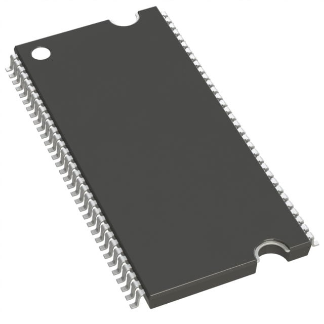
IC DRAM 256MBIT PARALLEL 66TSOP |
|---|---|
| Quantity | 518 Available (as of June 15, 2026) |

| Product Category | Memory |
|---|---|
| Manufacturer | Micron Technology Inc. |
| Manufacturing Status | Obsolete |
| Manufacturer Standard Lead Time | Contact Us |
| Datasheet |
Specifications & Environmental
| Device Package | 66-TSOP | Memory Format | DRAM | Technology | SDRAM - DDR | ||
|---|---|---|---|---|---|---|---|
| Memory Size | 256 Mbit | Access Time | 700 ps | Grade | Commercial | ||
| Clock Frequency | 200 MHz | Voltage | 2.5V ~ 2.7V | Memory Type | Volatile | ||
| Operating Temperature | 0°C ~ 70°C (TA) | Write Cycle Time Word Page | 15 ns | Packaging | 66-TSSOP (0.400", 10.16mm Width) | ||
| Mounting Method | Volatile | Memory Interface | Parallel | Memory Organization | 32M x 8 | ||
| Moisture Sensitivity Level | 3 (168 Hours) | RoHS Compliance | ROHS3 Compliant | REACH Compliance | REACH Unaffected | ||
| Qualification | N/A | ECCN | EAR99 | HTS Code | 8542.32.0024 |
Overview of MT46V32M8P-5B:GTR – IC DRAM 256MBIT PARALLEL 66TSOP
The MT46V32M8P-5B:GTR is a 256 Mbit DDR SDRAM organized as 32M × 8 with a parallel memory interface in a 66‑TSSOP package. It implements a double-data-rate (DDR) architecture with on‑die DLL and bidirectional data strobe (DQS) to support source‑synchronous data capture.
Designed for board‑level integration where compact TSOP packaging and standard 2.5 V I/O are required, the device targets systems that need low-voltage DDR memory with programmable burst lengths, internal banked operation and commercial temperature operation (0 °C to +70 °C).
Key Features
- Core Architecture Internal pipelined DDR architecture providing two data accesses per clock cycle; differential clock inputs (CK/CK#) and on‑die DLL for timing alignment.
- Memory Organization 256 Mbit capacity organized as 32M × 8 with four internal banks to support concurrent operations and efficient bank interleaving.
- Timing & Performance Specified for a 200 MHz clock frequency (speed grade -5B) with an access time of 700 ps and programmable burst lengths of 2, 4 or 8.
- Data Integrity & Strobes Bidirectional data strobe (DQS) transmitted/received with data for source‑synchronous capture; data mask (DM) supported for write masking.
- Refresh & Self‑Refresh Auto refresh with 8K refresh cycles; commercial refresh period 64 ms / 8192 cycles. Self‑refresh option noted in datasheet (availability varies by option).
- Voltage & I/O VDD/VDDQ supply range specified at 2.5 V ± tolerances (2.5 V ~ 2.7 V per device data); 2.5 V I/O (SSTL_2‑compatible) signaling.
- Package & Mounting 66‑pin TSSOP (0.400", 10.16 mm width) plastic TSOP package for board‑level mounting and compact footprint.
- Operating Range Commercial temperature rating: 0 °C to +70 °C (TA) as specified for this part.
Typical Applications
- Board‑level memory expansion Use as parallel DDR SDRAM for systems requiring compact TSOP memory devices with standard 2.5 V I/O.
- Timing‑sensitive data buffering Source‑synchronous DQS and on‑die DLL support read/write timing alignment in designs with tight timing windows.
- Systems requiring banked memory operations Four internal banks enable concurrent memory operations and improved throughput for multi‑access workloads.
Unique Advantages
- Double‑data‑rate operation: Internal DDR architecture enables two data transfers per clock cycle, increasing data throughput without increasing clock rate.
- Precise timing alignment: On‑die DLL and bidirectional DQS provide controlled alignment of DQ/DQS transitions with CK, aiding reliable source‑synchronous capture.
- Flexible burst operation: Programmable burst lengths (2, 4, 8) allow tuning of transfer granularity for different access patterns and system requirements.
- Standard 2.5 V I/O compatibility: VDD/VDDQ supply and SSTL_2‑compatible I/O simplify integration with 2.5 V system interfaces.
- Compact TSOP package: 66‑TSSOP footprint (10.16 mm width) provides a space‑efficient solution for board designs requiring a parallel DDR device.
- Commercial temperature support: Rated for 0 °C to +70 °C operation for standard commercial applications.
Why Choose IC DRAM 256MBIT PARALLEL 66TSOP?
The MT46V32M8P-5B:GTR offers a verified DDR SDRAM implementation with on‑die DLL, DQS support and four internal banks in a compact 66‑TSSOP package. Its 32M × 8 organization, programmable burst lengths and 2.5 V I/O make it suitable for designs that require parallel DDR memory with controlled timing and a standard voltage interface.
This device is appropriate for engineers and procurement teams seeking a commercial‑temperature DDR memory device that balances density, timing features and a compact board footprint for system‑level memory integration.
Request a quote or submit a pricing inquiry to receive availability and lead‑time information for the MT46V32M8P-5B:GTR.