MT46V32M8TG-5B:G TR
| Part Description |
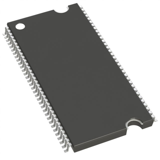
IC DRAM 256MBIT PARALLEL 66TSOP |
|---|---|
| Quantity | 1,582 Available (as of June 15, 2026) |

| Product Category | Memory |
|---|---|
| Manufacturer | Micron Technology Inc. |
| Manufacturing Status | Obsolete |
| Manufacturer Standard Lead Time | Contact Us |
| Datasheet |
Specifications & Environmental
| Device Package | 66-TSOP | Memory Format | DRAM | Technology | SDRAM - DDR | ||
|---|---|---|---|---|---|---|---|
| Memory Size | 256 Mbit | Access Time | 700 ps | Grade | Commercial | ||
| Clock Frequency | 200 MHz | Voltage | 2.5V ~ 2.7V | Memory Type | Volatile | ||
| Operating Temperature | 0°C ~ 70°C (TA) | Write Cycle Time Word Page | 15 ns | Packaging | 66-TSSOP (0.400", 10.16mm Width) | ||
| Mounting Method | Volatile | Memory Interface | Parallel | Memory Organization | 32M x 8 | ||
| Moisture Sensitivity Level | 2 (1 Year) | RoHS Compliance | RoHS non-compliant | REACH Compliance | REACH Unaffected | ||
| Qualification | N/A | ECCN | EAR99 | HTS Code | 8542.32.0024 |
Overview of MT46V32M8TG-5B:G TR – IC DRAM 256Mbit Parallel 66-TSSOP
The MT46V32M8TG-5B:G TR is a 256 Mbit DDR SDRAM device organized as 32M × 8 with a parallel memory interface in a 66-pin TSSOP package. It implements a double-data-rate architecture with internal pipelining and supports source-synchronous data capture for high-throughput memory transfers.
This device is intended for commercial-temperature (0°C to 70°C) systems that require a 2.5 V I/O DDR memory solution in a compact 66-TSSOP footprint, offering 200 MHz clock operation with two data transfers per clock cycle.
Key Features
- Core / Architecture
Double Data Rate (DDR) SDRAM with internal pipelined DDR architecture performing two data accesses per clock cycle and an internal DLL to align DQ/DQS with CK. - Memory Organization & Size
256 Mbit capacity, organized as 32M × 8 with four internal banks for concurrent operation. - Timing & Performance
Supports 200 MHz clock frequency (DDR operation) with an access time of 700 ps and write cycle time (word page) of 15 ns; -5B timing grade shown for 5 ns cycle at CL = 3. - Data I/O and Strobe
Bidirectional data strobe (DQS) transmitted/received with data for source-synchronous capture; DQS edge-aligned for READs and center-aligned for WRITEs. - Clock & Command
Differential clock inputs (CK and CK#) with commands entered on positive CK edges. - Power
VDD/VDDQ supply range +2.5 V ±0.2 V (documented option also lists +2.6 V ±0.1 V for DDR400); 2.5 V I/O compatible with SSTL_2 signaling. - Programmable Features
Programmable burst lengths (2, 4, or 8), data mask (DM) for write masking, auto refresh and concurrent auto precharge options supported. - Package & Temperature
66‑pin TSSOP (0.400", 10.16 mm width) package; commercial operating temperature 0°C to +70°C.
Typical Applications
- Commercial embedded systems
Provides 256 Mbit DDR SDRAM in a compact 66-TSSOP package for board-level memory expansion in commercial-temperature electronic products. - Board-level memory subsystems
Parallel DDR interface and 32M × 8 organization suit designs that require straightforward memory mapping and source-synchronous data capture. - Legacy or space-constrained designs
66‑TSSOP package and standard 2.5 V I/O make this device suitable for systems retaining parallel DDR memory interfaces and tight PCB layouts.
Unique Advantages
- DDR source-synchronous capture
Bidirectional DQS and DLL alignment enable reliable DDR read/write timing and source-synchronous data transfers. - 200 MHz DDR operation
Supports 200 MHz clocking for doubled data throughput per clock cycle (DDR mode) as specified for the -5B timing grade. - SSTL_2-compatible I/O
2.5 V I/O levels provide compatibility with SSTL_2 signaling standards noted in the datasheet. - Flexible burst and refresh control
Programmable burst lengths, auto refresh, and concurrent auto precharge options allow tuning for varied access patterns and system refresh requirements. - Compact, reliable package
Longer‑lead 66‑TSSOP (OCPL) option is documented for improved reliability in board-level assemblies.
Why Choose IC DRAM 256MBIT PARALLEL 66TSOP?
The MT46V32M8TG-5B:G TR offers a 256 Mbit DDR SDRAM solution with documented 200 MHz operation, source-synchronous DQS handling, and 2.5 V SSTL_2-compatible I/O in a 66‑pin TSSOP package. Its four-bank DDR architecture, programmable burst lengths, and on-die DLL make it suitable for commercial designs that require deterministic parallel DDR memory behavior and compact package integration.
This device is appropriate for engineers specifying commercial-temperature board-level DDR memory where a 32M × 8 organization, 2.5 V supply, and a 66‑TSSOP footprint are required; the documented timing grade (-5B) and timing parameters support designs targeting DDR transfer rates at the stated clock frequency.
If you would like a quote or need pricing and availability details for MT46V32M8TG-5B:G TR, please request a quote or submit a purchase inquiry and include your required quantity and delivery timeline.