MT46V32M8TG-75 IT:G
| Part Description |
IC DRAM 256MBIT PARALLEL 66TSOP |
|---|---|
| Quantity | 148 Available (as of June 15, 2026) |

| Product Category | Memory |
|---|---|
| Manufacturer | Micron Technology Inc. |
| Manufacturing Status | Obsolete |
| Manufacturer Standard Lead Time | Contact Us |
| Datasheet |
Specifications & Environmental
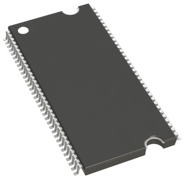
| Device Package | 66-TSOP | Memory Format | DRAM | Technology | SDRAM - DDR | ||
|---|---|---|---|---|---|---|---|
| Memory Size | 256 Mbit | Access Time | 750 ps | Grade | Industrial | ||
| Clock Frequency | 133 MHz | Voltage | 2.3V ~ 2.7V | Memory Type | Volatile | ||
| Operating Temperature | -40°C ~ 85°C (TA) | Write Cycle Time Word Page | 15 ns | Packaging | 66-TSSOP (0.400", 10.16mm Width) | ||
| Mounting Method | Volatile | Memory Interface | Parallel | Memory Organization | 32M x 8 | ||
| Moisture Sensitivity Level | 2 (1 Year) | RoHS Compliance | RoHS non-compliant | REACH Compliance | REACH Unaffected | ||
| Qualification | N/A | ECCN | EAR99 | HTS Code | 8542.32.0024 |
Overview of MT46V32M8TG-75 IT:G – IC DRAM 256MBIT PARALLEL 66TSOP
The MT46V32M8TG-75 IT:G is a 256 Mbit DDR SDRAM organized as 32M × 8 with a parallel memory interface in a 66‑TSSOP package. It implements an internal, pipelined double‑data‑rate architecture that provides two data accesses per clock cycle and supports source‑synchronous data capture.
Designed for systems that require volatile, board‑level DDR memory with defined timing options and an industrial operating temperature range, this device delivers compact package integration, selectable burst lengths, and standard 2.5 V I/O signaling.
Key Features
- Core Architecture Internal pipelined DDR architecture enabling two data accesses per clock cycle and a DLL to align DQ/DQS transitions with CK.
- Memory Organization & Capacity 256 Mbit total capacity, organized as 32M × 8 with four internal banks for concurrent operation.
- Performance & Timing 133 MHz clock frequency (DDR), 750 ps access time, and programmable burst lengths of 2, 4, or 8 for flexible data transfer patterns.
- Data Integrity & Capture Bidirectional data strobe (DQS) transmitted/received with data for source‑synchronous capture and data mask (DM) support for masking write data.
- Interface & Signaling Differential clock inputs (CK, CK#) and 2.5 V I/O (SSTL_2‑compatible) operation; commands entered on positive CK edge.
- Power Supply voltage range VDD/VDDQ = 2.3 V to 2.7 V (VDD = +2.5 V ±0.2 V typical).
- Package & Mounting 66‑TSSOP package (0.400" / 10.16 mm width) intended for board‑level mounting.
- Temperature Range Industrial rating: –40°C to +85°C (TA).
Typical Applications
- Board‑level memory expansion Compact 66‑TSSOP package and 256 Mbit density suited for adding parallel DDR memory to system PCBs.
- Industrial control and automation Industrial temperature rating (–40°C to +85°C) makes the device suitable for memory in control systems operating across a wide temperature range.
- Timing‑sensitive data buffering Source‑synchronous DQS and DLL alignment support reliable read/write timing for latency‑sensitive buffering tasks.
- Volatile storage for parallel DDR designs DDR operation with programmable burst lengths enables flexible data transfer modes in parallel interface architectures.
Unique Advantages
- Double‑data‑rate throughput: Two data accesses per clock cycle (DDR) increase effective data bandwidth compared with single‑rate DRAM at the same clock frequency.
- Source‑synchronous capture: Bidirectional DQS with DLL alignment improves read/write timing margins and data integrity.
- Flexible timing configuration: Programmable burst lengths (2/4/8) and defined speed grade timing options provide adaptability to different system throughput and latency requirements.
- Industrial temperature support: –40°C to +85°C rating enables use in temperature‑challenging environments.
- Standard 2.5 V signaling: SSTL_2‑compatible I/O and VDD/VDDQ range of 2.3 V–2.7 V ensure compatibility with 2.5 V system interfaces.
- Compact board footprint: 66‑TSSOP (10.16 mm width) package for high‑density board implementations.
Why Choose MT46V32M8TG-75 IT:G?
The MT46V32M8TG-75 IT:G provides a defined 256 Mbit DDR SDRAM option with source‑synchronous DQS, DLL timing alignment, and programmable burst lengths for flexible, timing‑sensitive parallel memory implementations. Its industrial temperature rating and compact 66‑TSSOP package make it suitable for systems that require reliable volatile storage in space‑constrained board designs.
This device is appropriate for designers specifying a 32M × 8, 4‑bank DDR memory with 2.5 V I/O and explicit timing parameters (133 MHz clock frequency, 750 ps access time). Use it where predictable DDR timing, compact packaging, and industrial temperature capability are primary selection criteria.
Request a quote or submit an inquiry to receive pricing, availability, and lead‑time information for MT46V32M8TG-75 IT:G.