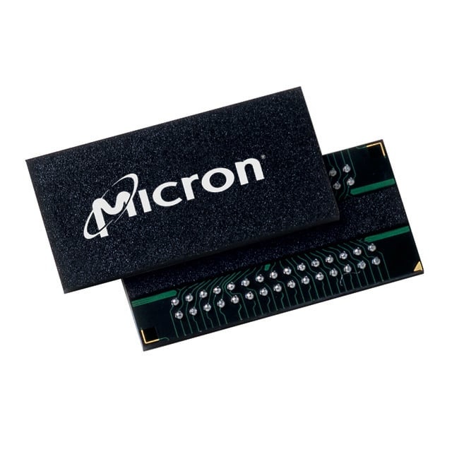
MT46V64M8BN-5B:F
| Part Description |
IC DRAM 512MBIT PARALLEL 60FBGA |
|---|---|
| Quantity | 163 Available (as of June 10, 2026) |

| Product Category | Memory |
|---|---|
| Manufacturer | Micron Technology Inc. |
| Manufacturing Status | Obsolete |
| Manufacturer Standard Lead Time | Contact Us |
| Datasheet |
Specifications & Environmental
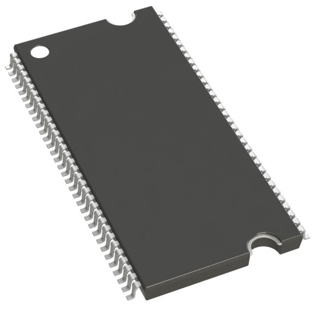
| Device Package | 60-FBGA (10x12.5) | Memory Format | DRAM | Technology | SDRAM - DDR | ||
|---|---|---|---|---|---|---|---|
| Memory Size | 512 Mbit | Access Time | 700 ps | Grade | Commercial | ||
| Clock Frequency | 200 MHz | Voltage | 2.5V ~ 2.7V | Memory Type | Volatile | ||
| Operating Temperature | 0°C ~ 70°C (TA) | Write Cycle Time Word Page | 15 ns | Packaging | 60-TFBGA | ||
| Mounting Method | Volatile | Memory Interface | Parallel | Memory Organization | 64M x 8 | ||
| Moisture Sensitivity Level | 5 (48 Hours) | RoHS Compliance | RoHS non-compliant | REACH Compliance | REACH Unaffected | ||
| Qualification | N/A | ECCN | EAR99 | HTS Code | 8542.32.0024 |
Overview of MT46V64M8BN-5B:F – 512Mbit DDR SDRAM, 60‑FBGA
The MT46V64M8BN-5B:F is a 512 Mbit parallel DDR SDRAM in a 60‑ball FBGA package. It implements a pipelined double-data-rate architecture with a 64M × 8 organization and a parallel memory interface for high‑throughput board‑level memory.
Designed for systems requiring DDR performance at up to 200 MHz clock rate, the device offers programmable burst lengths, internal DLL alignment, and standard 2.5 V I/O to support common DDR timing and interface requirements while fitting a compact 10 mm × 12.5 mm FBGA footprint.
Key Features
- Core / Architecture Internal, pipelined double‑data‑rate (DDR) architecture providing two data accesses per clock cycle and a DLL to align DQ/DQS with CK.
- Memory Organization 512 Mbit capacity organized as 64M × 8 with four internal banks for concurrent operation.
- Clock and Timing Rated to a 200 MHz clock frequency (speed grade -5B); datasheet timing characteristics include a data‑out window and DQS/DQ skew specifications for source‑synchronous capture.
- Performance Metrics Access time ~700 ps and a word/page write cycle time of 15 ns (device timing per datasheet).
- Power and I/O VDD/VDDQ supply range specified at 2.5 V ± tolerances (device options include DDR400 VDD variants); I/O uses 2.5 V signalling.
- Interface and Data Integrity Differential clock inputs (CK/CK#), bidirectional data strobe (DQS), and data mask (DM) support source‑synchronous reads/writes and masked writes.
- Memory Management Programmable burst lengths (2, 4, or 8), auto refresh (8K refresh cycle), concurrent auto precharge option and support for self refresh (not available on AT devices as noted in the datasheet).
- Package and Thermal 60‑ball FBGA package (10 mm × 12.5 mm), part marking BN indicates Pb‑free FBGA option; commercial operating temperature 0°C to 70°C (TA).
Typical Applications
- PC memory subsystems — Speed grade compatibility and timing options map to common PC DDR speed classes, making the device suitable for designs targeting those timing families.
- Compact board‑level DDR memory — 60‑ball FBGA (10 mm × 12.5 mm) package provides a small footprint for space‑constrained system boards.
- Systems requiring 2.5 V DDR I/O — Standard 2.5 V VDD/VDDQ levels and source‑synchronous DQS/CK interface support typical 2.5 V DDR signaling environments.
Unique Advantages
- Double data‑rate throughput: Two data transfers per clock cycle multiply effective bandwidth while retaining a parallel DDR interface.
- Flexible timing options: -5B speed grade with documented timing windows and DQS/DQ skew data supports deterministic timing design and signal integrity planning.
- Compact, Pb‑free FBGA: 60‑ball FBGA (10 mm × 12.5 mm) package offers board‑level density with Pb‑free package option (BN marking).
- On‑chip refresh and bank architecture: Four internal banks plus auto refresh and programmable burst lengths enable concurrent operations and simplified refresh management.
- Standard 2.5 V I/O: Compatible with SSTL_2‑style 2.5 V signaling as documented in the device features, easing interface design with common DDR controllers.
Why Choose MT46V64M8BN-5B:F?
The MT46V64M8BN-5B:F is positioned for designs that require a compact, board‑level 512 Mbit DDR SDRAM with documented timing, source‑synchronous DQS support, and a 60‑ball FBGA footprint. Its DDR architecture, programmable burst lengths, and internal bank structure provide predictable performance for systems targeting 2.5 V DDR timing classes.
This device is suitable for engineers specifying parallel DDR memory where small package size, defined timing parameters (including a 200 MHz clock option), and standard 2.5 V I/O are required. The datasheet contains full timing and electrical details to support system integration and long‑term design validation.
For pricing, availability, or to request a quote for MT46V64M8BN-5B:F, please submit a sales inquiry or quote request with your quantity and delivery requirements.