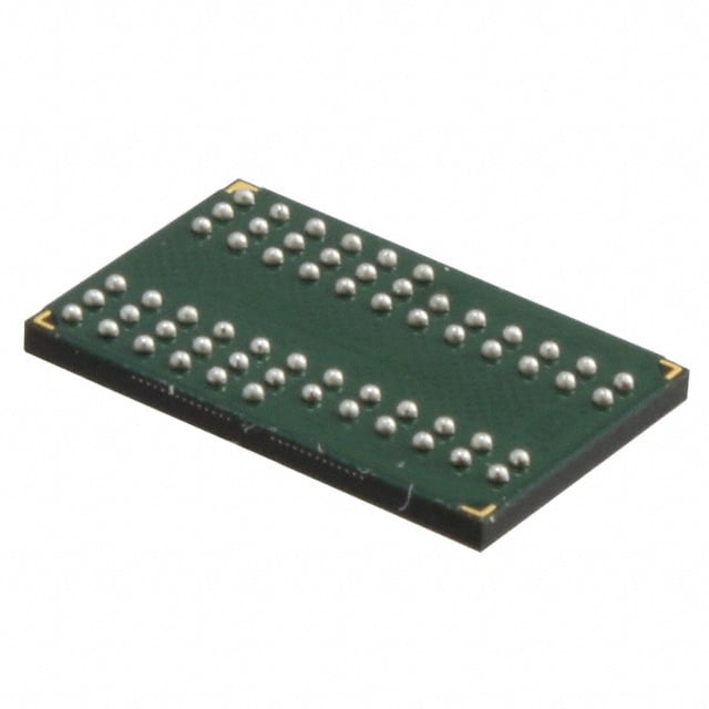
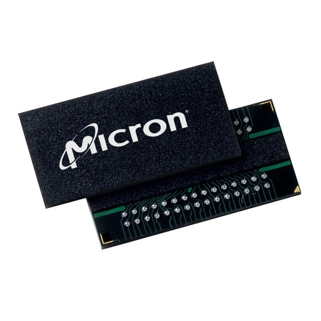
MT46V64M8BN-6:F
| Part Description |
IC DRAM 512MBIT PAR 60FBGA |
|---|---|
| Quantity | 951 Available (as of June 9, 2026) |

| Product Category | Memory |
|---|---|
| Manufacturer | Micron Technology Inc. |
| Manufacturing Status | Obsolete |
| Manufacturer Standard Lead Time | Contact Us |
| Datasheet |
Specifications & Environmental
| Device Package | 60-FBGA (10x12.5) | Memory Format | DRAM | Technology | SDRAM - DDR | ||
|---|---|---|---|---|---|---|---|
| Memory Size | 512 Mbit | Access Time | 700 ps | Grade | Commercial | ||
| Clock Frequency | 167 MHz | Voltage | 2.3V ~ 2.7V | Memory Type | Volatile | ||
| Operating Temperature | 0°C ~ 70°C (TA) | Write Cycle Time Word Page | 15 ns | Packaging | 60-TFBGA | ||
| Mounting Method | Volatile | Memory Interface | Parallel | Memory Organization | 64M x 8 | ||
| Moisture Sensitivity Level | 5 (48 Hours) | RoHS Compliance | RoHS non-compliant | REACH Compliance | REACH Unaffected | ||
| Qualification | N/A | ECCN | EAR99 | HTS Code | 8542.32.0024 |
Overview of MT46V64M8BN-6:F – IC DRAM 512MBIT PAR 60FBGA
The MT46V64M8BN-6:F is a 512 Mbit volatile DDR SDRAM organized as 64M × 8 with a parallel memory interface. It implements internal pipelined double-data-rate architecture with source-synchronous DQS and differential clock inputs to support high-throughput data transfer.
Targeted for board-level memory integration, the device combines a compact 60-ball TFBGA package with commercial operating range and low-voltage operation to address space-constrained designs requiring DDR performance at a 167 MHz clock rate (speed grade -6).
Key Features
- Core / Architecture Internal pipelined DDR architecture providing two data transfers per clock cycle and a DLL to align DQ/DQS transitions with CK.
- Memory Organization & Capacity 512 Mbit total capacity, organized as 64M × 8 with four internal banks (16 Meg × 8 × 4 banks as specified).
- Performance & Timing Clock frequency up to 167 MHz (speed grade -6) with an access time of 700 ps and write cycle time (word page) of 15 ns.
- Data Interface Parallel memory interface with bidirectional data strobe (DQS) transmitted/received with data; DQS is edge-aligned for READs and center-aligned for WRITEs.
- Programmable Operation Programmable burst lengths of 2, 4 or 8 and support for auto precharge and concurrent auto precharge operation.
- Power Supply range specified at 2.3 V to 2.7 V for device operation.
- Package 60-ball TFBGA / FBGA (10 mm × 12.5 mm) compact package for high-density board mounting.
- Temperature Range Commercial operating temperature: 0 °C to +70 °C (TA) as specified.
- Additional DDR Features Differential clock inputs (CK/CK#), data mask (DM), and support for multiple timing grades listed in the datasheet.
Typical Applications
- Module and system memory Use as a 512 Mbit DDR SDRAM device in parallel memory interfaces where a 64M × 8 organization and four-bank operation are required.
- PC speed-grade memory Speed-grade compatibility information in the datasheet includes PC3200, PC2700 and PC2100 listings for applicable timing grades.
- Compact board-level memory 60-ball FBGA (10 × 12.5 mm) package supports high-density board layouts and compact module designs.
Unique Advantages
- DDR source-synchronous capture: Bidirectional DQS with DLL alignment enables reliable data capture for both reads and writes, supporting consistent timing behavior.
- High effective bandwidth per clock: Double-data-rate architecture provides two data transfers per clock cycle, increasing throughput without raising core clock frequency.
- Compact, board-friendly package: 60-ball FBGA (10 × 12.5 mm) minimizes PCB footprint for space-constrained designs.
- Flexible timing options: Datasheet specifies multiple speed/timing grades and programmable burst lengths (2/4/8) to match system latency and throughput requirements.
- Standard commercial temperature rating: Specified for 0 °C to +70 °C operation for use in commercial applications.
- Low-voltage operation: 2.3 V to 2.7 V supply range supports lower-power system designs compared to legacy higher-voltage memories.
Why Choose IC DRAM 512MBIT PAR 60FBGA?
The MT46V64M8BN-6:F positions itself as a compact, 512 Mbit DDR SDRAM element suitable for designs that require DDR transfer efficiency, a parallel interface and a small-footprint FBGA package. Its combination of four internal banks, programmable burst lengths and source-synchronous DQS supports predictable timing and throughput in board-level memory subsystems.
This device is appropriate for commercial-temperature applications that need a 64M × 8 memory organization, a 167 MHz clock speed grade, and a low-voltage supply range. Its documented timing grades and package dimensions make it a practical choice for engineers integrating DDR SDRAM where space and timing control are key considerations.
Request a quote or submit an inquiry for pricing, availability and lead-time information for the MT46V64M8BN-6:F.