MT46V64M8FN-5B:D TR
| Part Description |
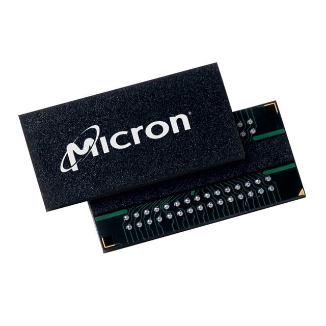
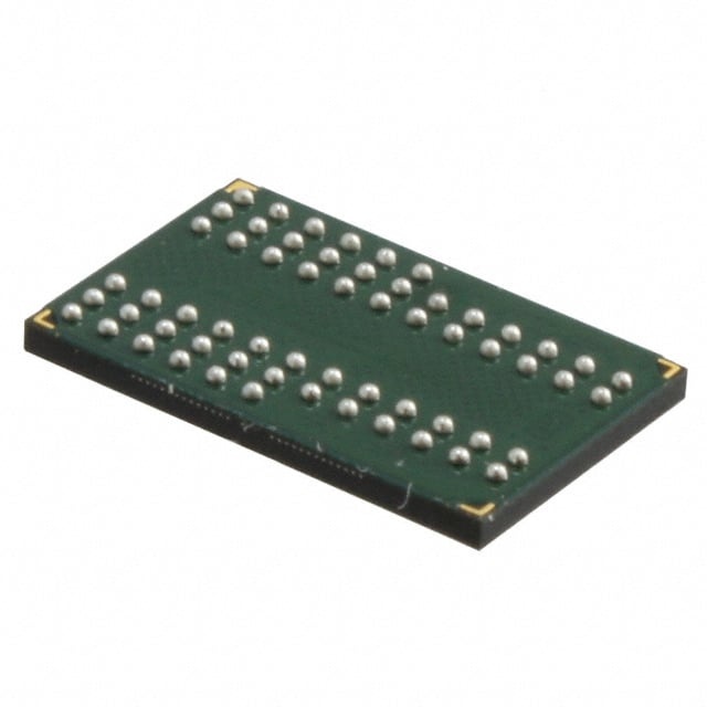
IC DRAM 512MBIT PARALLEL 60FBGA |
|---|---|
| Quantity | 583 Available (as of June 15, 2026) |

| Product Category | Memory |
|---|---|
| Manufacturer | Micron Technology Inc. |
| Manufacturing Status | Obsolete |
| Manufacturer Standard Lead Time | Contact Us |
| Datasheet |
Specifications & Environmental
| Device Package | 60-FBGA (10x12.5) | Memory Format | DRAM | Technology | SDRAM - DDR | ||
|---|---|---|---|---|---|---|---|
| Memory Size | 512 Mbit | Access Time | 700 ps | Grade | Commercial | ||
| Clock Frequency | 200 MHz | Voltage | 2.5V ~ 2.7V | Memory Type | Volatile | ||
| Operating Temperature | 0°C ~ 70°C (TA) | Write Cycle Time Word Page | 15 ns | Packaging | 60-TFBGA | ||
| Mounting Method | Volatile | Memory Interface | Parallel | Memory Organization | 64M x 8 | ||
| Moisture Sensitivity Level | 5 (48 Hours) | RoHS Compliance | N/A | REACH Compliance | REACH Unaffected | ||
| Qualification | N/A | ECCN | EAR99 | HTS Code | 8542.32.0024 |
Overview of MT46V64M8FN-5B:D TR – IC DRAM 512Mbit Parallel 60FBGA
The MT46V64M8FN-5B:D TR is a 512 Mbit DDR SDRAM device organized as 64M × 8 with a parallel memory interface in a 60-ball FBGA (10 mm × 12.5 mm) package. It implements a double-data-rate architecture with source-synchronous DQS signaling and an internal DLL to support two data transfers per clock.
This device targets systems that require 512 Mbit of volatile DDR memory with 2.5 V I/O and commercial temperature operation (0 °C to 70 °C). Key value comes from its DDR performance (200 MHz clock rate for the -5B timing grade), compact FBGA footprint, and standard DDR features such as programmable burst lengths and internal banked architecture.
Key Features
- Core / DDR Architecture Internal pipelined DDR architecture providing two data accesses per clock cycle; DLL aligns DQ and DQS transitions with CK for reliable source-synchronous transfers.
- Memory Organization 512 Mbit total capacity configured as 64M × 8 (16 Meg × 8 × 4 banks), enabling banked operation and concurrent accesses across four internal banks.
- Performance & Timing -5B speed grade supports a 200 MHz clock rate (DDR data rate) with a reported data-out window and access characteristics; access time listed as 700 ps.
- Data Strobe and Mask Bidirectional data strobe (DQS) transmitted/received with data; data mask (DM) supported for masked writes.
- Clock & Command Differential clock inputs (CK and CK#) with commands entered on positive CK edges to support standard DDR timing models.
- Programmable Burst & Refresh Programmable burst lengths of 2, 4, or 8; supports auto refresh and self refresh options as indicated in the datasheet.
- Power & I/O VDD / VDDQ supply range specified at 2.5 V ± tolerance (device data lists VDD = +2.5 V ±0.2 V and DDR400 option at +2.6 V ±0.1 V); 2.5 V I/O is SSTL_2 compatible.
- Package & Temperature 60-ball FBGA (10 mm × 12.5 mm) supplier device package; commercial operating temperature range 0 °C to +70 °C.
Typical Applications
- DDR memory subsystems Use as onboard parallel DDR SDRAM for systems that require 512 Mbit of volatile memory with standard DDR signaling and SSTL_2-compatible I/O.
- PC DDR compatibility scenarios Device timing grades and the datasheet’s speed-grade compatibility table reference PC3200 / PC2700 / PC2100 timing categories, indicating suitability where those DDR timing classes are required.
- Compact boards with FBGA constraints 60-ball FBGA (10 mm × 12.5 mm) package supports compact PCB layouts where a small, low-profile DDR device is required.
Unique Advantages
- DDR double-data-rate throughput: Two data transfers per clock via internal pipelined DDR architecture increases effective bandwidth at an available 200 MHz clock rate for the -5B grade.
- Banked memory for concurrent access: Four internal banks (BA0, BA1) permit overlapping operations to improve effective access concurrency.
- SSTL_2-compatible 2.5 V I/O: VDDQ specified at 2.5 V (with documented tolerances) aligns with SSTL_2 signaling requirements for standard DDR interfaces.
- Flexible burst and refresh controls: Programmable burst lengths (2, 4, 8) plus auto-refresh and optional self-refresh support a range of transfer patterns and power/refresh strategies.
- Compact FBGA footprint: 60-ball FBGA (10 mm × 12.5 mm) package reduces PCB area while delivering a 512 Mbit DDR solution.
- Well-documented timing grades: -5B timing grade provides defined timing windows (including data-out window and DQS–DQ skew) to assist signal integrity and timing closure.
Why Choose IC DRAM 512MBIT PARALLEL 60FBGA?
The MT46V64M8FN-5B:D TR provides a compact, standards-oriented 512 Mbit DDR SDRAM option for designs that require parallel DDR memory with 2.5 V I/O and a 60-ball FBGA footprint. Its banked DDR architecture, programmable burst lengths, and documented timing grades give designers measurable parameters for performance and timing closure.
This device is suited to projects needing a commercial-temperature (0 °C to +70 °C) DDR memory component with Micron’s documented DDR features (DQS, DLL, differential clocks) and 2.5 V supply operation. The datasheet-backed specifications make it a practical choice for integrating 512 Mbit DDR into space-constrained boards that rely on SSTL_2-compatible signaling and standard DDR timing categories.
Request a quote or submit a parts inquiry to obtain pricing and lead-time information for MT46V64M8FN-5B:D TR.