MT46V64M8CY-5B L:J
| Part Description |
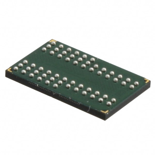
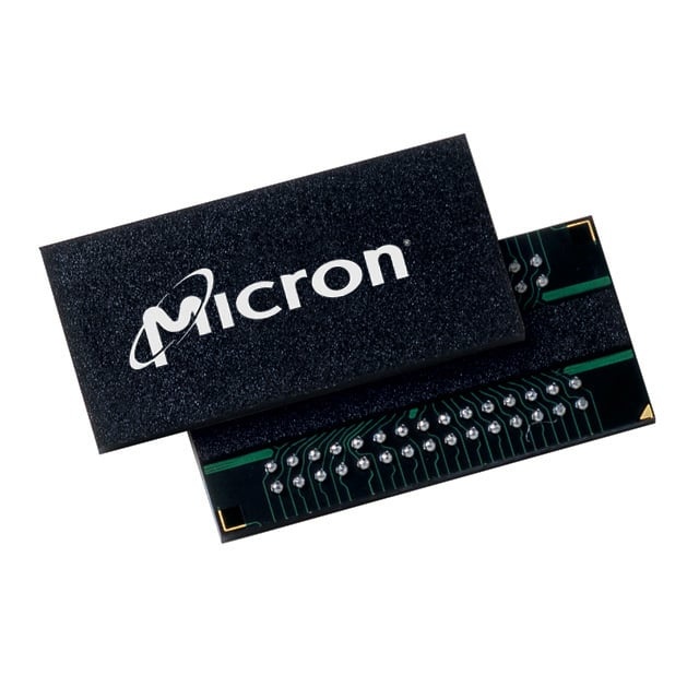
IC DRAM 512MBIT PARALLEL 60FBGA |
|---|---|
| Quantity | 369 Available (as of June 9, 2026) |

| Product Category | Memory |
|---|---|
| Manufacturer | Micron Technology Inc. |
| Manufacturing Status | Obsolete |
| Manufacturer Standard Lead Time | Contact Us |
| Datasheet |
Specifications & Environmental
| Device Package | 60-FBGA (8x12.5) | Memory Format | DRAM | Technology | SDRAM - DDR | ||
|---|---|---|---|---|---|---|---|
| Memory Size | 512 Mbit | Access Time | 700 ps | Grade | Commercial | ||
| Clock Frequency | 200 MHz | Voltage | 2.5V ~ 2.7V | Memory Type | Volatile | ||
| Operating Temperature | 0°C ~ 70°C (TA) | Write Cycle Time Word Page | 15 ns | Packaging | 60-TFBGA | ||
| Mounting Method | Volatile | Memory Interface | Parallel | Memory Organization | 64M x 8 | ||
| Moisture Sensitivity Level | 3 (168 Hours) | RoHS Compliance | ROHS3 Compliant | REACH Compliance | REACH Unaffected | ||
| Qualification | N/A | ECCN | EAR99 | HTS Code | 8542.32.0028 |
Overview of MT46V64M8CY-5B L:J – IC DRAM 512MBIT PARALLEL 60FBGA
The MT46V64M8CY-5B L:J is a 512 Mbit DDR SDRAM organized as 64M × 8 with a parallel memory interface and volatile memory operation. The device implements an internal, pipelined double-data-rate architecture that provides two data accesses per clock cycle and supports source-synchronous data capture using bidirectional DQS.
Designed for systems requiring DDR memory at a 200 MHz clock rate (speed grade -5B), the device operates from a 2.5 V to 2.7 V supply range and is offered in a 60-ball thin fine-pitch BGA package (8.0 × 12.5 mm). The device is specified for commercial temperature operation from 0°C to 70°C.
Key Features
- Core / Architecture Internal, pipelined DDR architecture enabling two data accesses per clock cycle; includes a DLL to align DQ and DQS transitions with CK.
- Memory Organization & Capacity 512 Mbit total capacity configured as 64M × 8 with four internal banks for concurrent operation.
- Timing & Performance Clock frequency listed at 200 MHz (speed grade -5B) with an access time of 700 ps and a write cycle time (word page) of 15 ns. Programmable burst lengths of 2, 4, or 8 are supported.
- Data Interface & Signals Bidirectional data strobe (DQS) transmitted/received with data for source-synchronous capture; differential clock inputs (CK and CK#); commands entered on positive CK edges. Data mask (DM) supported for write masking.
- Power & Voltage VDD/VDDQ operation around 2.5 V (VDD = +2.5 V ±0.2 V noted in datasheet options); listed device supply range is 2.5 V to 2.7 V. 2.5 V I/O (SSTL_2 compatible) is documented.
- Refresh & Power Management Auto refresh and specified refresh counts (8K); self-refresh options are described in the datasheet.
- Package & Temperature 60-ball thin FBGA package (10.0 mm × 12.5 mm / listed supplier package 8 × 12.5) and commercial temperature rating of 0°C to +70°C.
Unique Advantages
- Double-data-rate throughput: Two data accesses per clock cycle enable higher effective data rates compared with single-data-rate memories.
- Source-synchronous DQS: Bidirectional DQS with DLL alignment improves data capture timing by aligning DQ/DQS transitions with CK.
- Flexible burst and timing options: Programmable burst lengths (2/4/8) and documented timing grades (including -5B at 200 MHz) allow tailoring performance to system timing requirements.
- SSTL_2-compatible I/O at 2.5 V: Standard 2.5 V I/O levels simplify interfacing with 2.5 V memory controllers and I/O subsystems.
- Compact FBGA footprint: 60-ball FBGA (10.0 mm × 12.5 mm) provides a small board footprint for space-constrained designs.
- Commercial temperature rating: Specified operation from 0°C to +70°C for standard commercial applications.
Why Choose IC DRAM 512MBIT PARALLEL 60FBGA?
The MT46V64M8CY-5B L:J provides a 512 Mbit DDR SDRAM building block with a pipelined DDR core, source-synchronous DQS, and programmable burst lengths—features that support high-throughput parallel memory interfaces at a 200 MHz clock rate. Its 2.5 V I/O compatibility and compact 60-ball FBGA package make it suitable for designs that require a standard DDR memory element within a constrained PCB area.
This device is appropriate for designs targeting commercial temperature ranges and needing a 64M × 8 DDR memory organization with four internal banks and documented timing grades. The combination of DDR architecture, DQS alignment, and standard 2.5 V operation provides deterministic timing characteristics useful for engineered memory subsystems.
Please request a quote or submit an RFQ to check availability, lead times, and pricing for the MT46V64M8CY-5B L:J.