MT46V64M8P-5B AIT:J TR
| Part Description |
IC DRAM 512MBIT PARALLEL 66TSOP |
|---|---|
| Quantity | 1,123 Available (as of June 15, 2026) |

| Product Category | Memory |
|---|---|
| Manufacturer | Micron Technology Inc. |
| Manufacturing Status | Obsolete |
| Manufacturer Standard Lead Time | Contact Us |
| Datasheet |
Specifications & Environmental
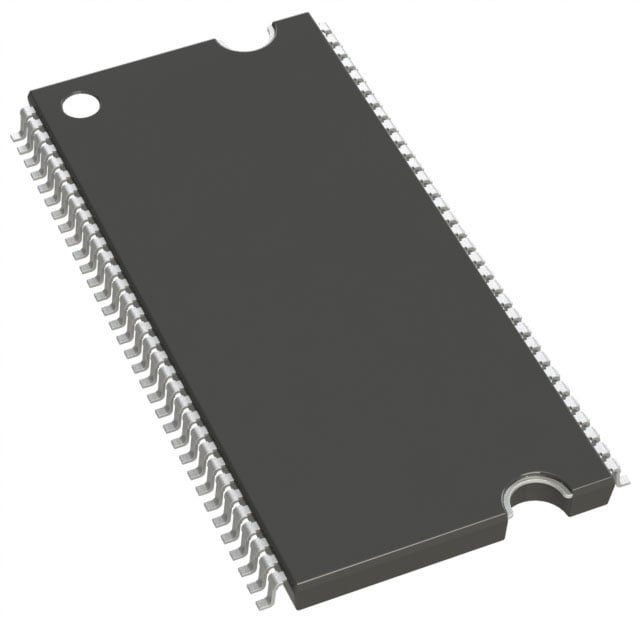
| Device Package | 66-TSOP | Memory Format | DRAM | Technology | SDRAM - DDR | ||
|---|---|---|---|---|---|---|---|
| Memory Size | 512 Mbit | Access Time | 700 ps | Grade | Automotive | ||
| Clock Frequency | 200 MHz | Voltage | 2.3V ~ 2.7V | Memory Type | Volatile | ||
| Operating Temperature | -40°C ~ 85°C (TA) | Write Cycle Time Word Page | 15 ns | Packaging | 66-TSSOP (0.400", 10.16mm Width) | ||
| Mounting Method | Volatile | Memory Interface | Parallel | Memory Organization | 64M x 8 | ||
| Moisture Sensitivity Level | 3 (168 Hours) | RoHS Compliance | ROHS3 Compliant | REACH Compliance | REACH Unaffected | ||
| Qualification | AEC-Q100 | ECCN | EAR99 | HTS Code | 8542.32.0036 |
Overview of MT46V64M8P-5B AIT:J TR – 512 Mbit DDR SDRAM, 66‑TSSOP
The MT46V64M8P-5B AIT:J TR is a 512 Mbit DDR SDRAM organized as 64M × 8 with a parallel memory interface. It implements an internal, pipelined double-data-rate (DDR) architecture for two data accesses per clock cycle and supports a 200 MHz clock rate for high-throughput parallel memory applications.
Targeted for automotive-grade systems, this device combines AEC‑Q100 qualification with a wide operating range and a compact 66‑TSSOP package, delivering verified reliability and a small footprint for constrained system designs that require DDR performance and automotive-grade qualification.
Key Features
- DDR architecture Internal pipelined double-data-rate operation provides two data transfers per clock cycle for improved throughput over single-data-rate memories.
- Memory organization & size 512 Mbit capacity organized as 64M × 8 with four internal banks to enable concurrent bank operation and flexible addressing.
- Performance Supports a 200 MHz clock frequency and an access time of 700 ps; key timing includes a write cycle time (word page) of 15 ns.
- Data strobes and timing Bidirectional data strobe (DQS) is transmitted/received with data for source‑synchronous capture; device includes an internal DLL to align DQ/DQS with CK.
- Flexible burst and masking Programmable burst lengths (2, 4, or 8) and data mask (DM) support controlled write masking and transfer granularity.
- Refresh and power options Auto refresh and self refresh options are supported; refresh timing variants include automotive timing options described in the device documentation.
- Supply and I/O Operates from a 2.3 V to 2.7 V supply range suitable for 2.5 V I/O signaling environments.
- Package 66‑pin TSSOP (0.400", 10.16 mm width) long‑lead TSOP option for improved reliability in board assembly and handling.
- Qualification and temperature AEC‑Q100 qualified and specified for an operating ambient temperature range of −40 °C to +85 °C (TA).
Typical Applications
- Automotive memory subsystems AEC‑Q100 qualification and −40 °C to +85 °C range make the device suitable for automotive electronic modules requiring DDR buffering or working memory.
- High-speed parallel buffering 200 MHz DDR operation and 64M × 8 organization support high-throughput parallel interface buffering in embedded controllers and digital subsystems.
- System-level data capture Source-synchronous DQS and programmable burst lengths enable reliable, deterministic data capture for timing-sensitive read/write operations.
Unique Advantages
- Automotive qualification (AEC‑Q100): Provides documented qualification for use in automotive-rated designs and environments.
- DDR throughput in compact package: Delivers double‑data‑rate performance in a 66‑TSSOP footprint to save PCB space without sacrificing speed.
- Robust timing features: Internal DLL, bidirectional DQS, and programmable burst lengths help simplify timing closure and improve data integrity.
- Wide supply tolerance: 2.3 V to 2.7 V supply range accommodates 2.5 V I/O systems and provides margin for system power variations.
- Concurrent bank operation: Four internal banks allow overlapping operations for improved effective bandwidth in multi-transaction workloads.
Why Choose MT46V64M8P-5B AIT:J TR?
The MT46V64M8P-5B AIT:J TR combines DDR performance, automotive qualification, and a compact 66‑TSSOP package to address space‑constrained designs that require verified reliability and deterministic timing. Its DDR architecture, DQS support and internal DLL simplify high-speed interface timing while the 64M × 8 organization and four internal banks provide flexible memory management.
This device is well suited to engineers designing automotive or high-reliability embedded systems that need a 512 Mbit parallel DDR memory solution with defined operating temperature range and supplier documentation for system integration and qualification.
Request a quote or submit a parts inquiry to receive pricing, lead-time, and availability information for MT46V64M8P-5B AIT:J TR. Provide your quantity and delivery requirements to expedite the response.