MT46V64M8P-5B:F
| Part Description |
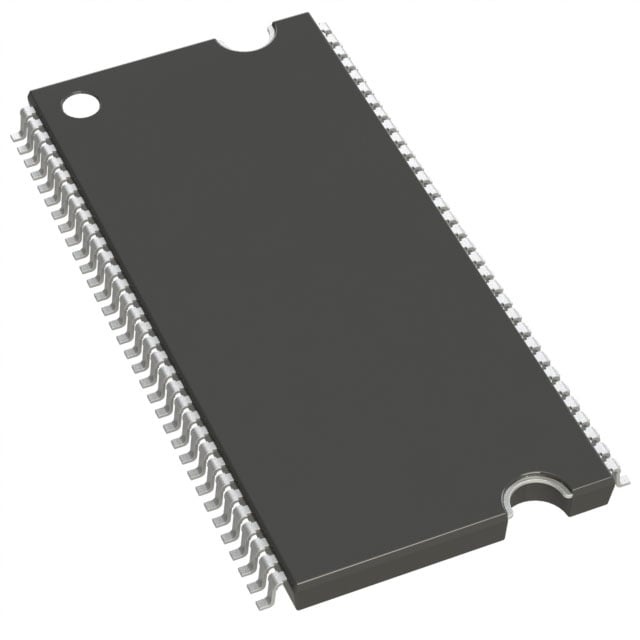
IC DRAM 512MBIT PARALLEL 66TSOP |
|---|---|
| Quantity | 704 Available (as of June 15, 2026) |

| Product Category | Memory |
|---|---|
| Manufacturer | Micron Technology Inc. |
| Manufacturing Status | Obsolete |
| Manufacturer Standard Lead Time | Contact Us |
| Datasheet |
Specifications & Environmental
| Device Package | 66-TSOP | Memory Format | DRAM | Technology | SDRAM - DDR | ||
|---|---|---|---|---|---|---|---|
| Memory Size | 512 Mbit | Access Time | 700 ps | Grade | Commercial | ||
| Clock Frequency | 200 MHz | Voltage | 2.5V ~ 2.7V | Memory Type | Volatile | ||
| Operating Temperature | 0°C ~ 70°C (TA) | Write Cycle Time Word Page | 15 ns | Packaging | 66-TSSOP (0.400", 10.16mm Width) | ||
| Mounting Method | Volatile | Memory Interface | Parallel | Memory Organization | 64M x 8 | ||
| Moisture Sensitivity Level | 5 (48 Hours) | RoHS Compliance | ROHS3 Compliant | REACH Compliance | REACH Unaffected | ||
| Qualification | N/A | ECCN | EAR99 | HTS Code | 8542.32.0024 |
Overview of MT46V64M8P-5B:F – IC DRAM 512MBIT PARALLEL 66TSOP
The MT46V64M8P-5B:F is a 512 Mbit DDR SDRAM organized as 64M x 8 with a parallel memory interface in a 66‑TSSOP package. It implements a dual-data-rate internal architecture with source‑synchronous DQS signaling and a DLL to align data with the clock for reliable high‑speed transfers.
This device is targeted at systems requiring a compact, parallel DDR memory solution operating at up to 200 MHz clock rate and a commercial temperature range, offering programmable burst lengths, auto‑refresh and standard DDR control features for board‑level memory expansion and legacy parallel DDR implementations.
Key Features
- Core Architecture Internal pipelined DDR architecture delivering two data accesses per clock cycle and a DLL to align DQ/DQS transitions with CK.
- Memory Organization & Capacity 512 Mbit capacity organized as 64M × 8 with four internal banks for concurrent operation.
- Performance & Timing Supports a clock frequency up to 200 MHz (speed grade -5B) with an access time of 700 ps and a word page write cycle time of 15 ns.
- Data Strobe & Mask Bidirectional data strobe (DQS) transmitted/received with data for source‑synchronous capture; includes data mask (DM) for selective write masking.
- Programmable Burst & Refresh Programmable burst lengths of 2, 4, or 8; supports auto refresh (64 ms, 8192 cycles for commercial devices) and self refresh options as specified in device options.
- Voltage & I/O VDD / VDDQ supply range 2.5 V to 2.7 V (SSTL_2 compatible I/O), aligning with standard DDR power domains.
- Interface & Clocks Differential clock inputs (CK, CK#) with commands entered on positive CK edges; DQS edge‑aligned for READs and center‑aligned for WRITEs.
- Package & Mounting 66‑TSSOP (0.400", 10.16 mm width) longer‑lead TSOP option for improved package reliability, suitable for board‑level mounting.
- Operating Range Commercial temperature rating: 0 °C to +70 °C (TA).
Typical Applications
- Board‑level Memory Expansion Provides 512 Mbit of parallel DDR memory in a compact 66‑TSSOP footprint for systems needing additional DRAM capacity.
- Embedded Systems Fits embedded platforms that use a parallel DDR interface and require standard commercial temperature operation.
- Legacy DDR Subsystems Suitable for designs that implement DDR SDRAM signaling with differential clocks and source‑synchronous DQS capture.
Unique Advantages
- DDR Source‑Synchronous Data Capture: Bidirectional DQS with DLL alignment reduces timing uncertainty and simplifies timing margins for high‑speed reads and writes.
- Flexible Burst and Bank Management: Programmable burst lengths (2/4/8) and four internal banks enable efficient data transfer patterns and improved throughput for bursty accesses.
- Compact TSOP Footprint: 66‑TSSOP package with longer leads offers a small board area and improved package handling reliability for surface‑mount applications.
- Standard DDR Voltage Domain: 2.5 V I/O (SSTL_2 compatible) and specified VDD/VDDQ range align with common DDR power architectures, facilitating integration.
- Commercial Temperature Qualification: Rated for 0 °C to +70 °C, matching many consumer and industrial electronic applications.
Why Choose MT46V64M8P-5B:F?
The MT46V64M8P-5B:F delivers a verified DDR SDRAM implementation in a compact 66‑TSSOP package, combining source‑synchronous DQS, DLL timing alignment and four internal banks to support reliable parallel DDR operation at up to 200 MHz. Its 512 Mbit density and 64M × 8 organization make it suitable for designs that require standard DDR features and a commercial temperature rating.
This device is appropriate for engineers specifying board‑level DRAM where a parallel DDR interface, programmable burst modes, and compact package mounting are required. Its defined timing parameters, refresh mechanisms and SSTL_2‑compatible I/O provide predictable integration into existing DDR memory subsystems.
If you would like pricing or availability, request a quote or submit a product inquiry and our team will respond with a tailored quote and lead‑time information.