MT46V64M8TG-5B IT:J TR
| Part Description |
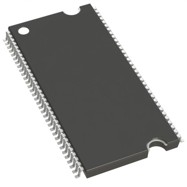
IC DRAM 512MBIT PARALLEL 66TSOP |
|---|---|
| Quantity | 1,214 Available (as of June 18, 2026) |

| Product Category | DRAM Memory |
|---|---|
| Manufacturer | Micron Technology Inc. |
| Manufacturing Status | Obsolete |
| Manufacturer Standard Lead Time | Contact Us |
| Datasheet |
Specifications & Environmental
| Device Package | 66-TSOP | Memory Format | DRAM | Technology | SDRAM - DDR | ||
|---|---|---|---|---|---|---|---|
| Memory Size | 512 Mbit | Access Time | 700 ps | Grade | Industrial | ||
| Clock Frequency | 200 MHz | Voltage | 2.5V ~ 2.7V | Memory Type | Volatile | ||
| Operating Temperature | -40°C ~ 85°C (TA) | Write Cycle Time Word Page | 15 ns | Packaging | 66-TSSOP (0.400", 10.16mm Width) | ||
| Mounting Method | Volatile | Memory Interface | Parallel | Memory Organization | 64M x 8 | ||
| Moisture Sensitivity Level | 3 (168 Hours) | RoHS Compliance | ROHS3 Compliant | REACH Compliance | REACH Unknown | ||
| Qualification | N/A | ECCN | EAR99 | HTS Code | 8542.32.0028 |
Overview of MT46V64M8TG-5B IT:J TR – IC DRAM 512MBIT PARALLEL 66TSOP
The MT46V64M8TG-5B IT:J TR is a 512 Mbit, x8 Double Data Rate (DDR) SDRAM offered in a 66‑pin TSSOP package. It implements an internal pipelined DDR architecture with four internal banks and a parallel memory interface optimized for systems requiring synchronous, source‑synchronous data capture.
Designed for commercial and industrial temperature operation, this device targets embedded and industrial applications that need a compact TSOP package, 2.5 V I/O, and DDR performance up to a 200 MHz clock frequency.
Key Features
- Core / Architecture Internal, pipelined Double‑Data‑Rate (DDR) SDRAM architecture providing two data transfers per clock cycle and four internal banks for concurrent operation.
- Memory Organization 512 Mbit density organized as 64M × 8, suitable for systems that require x8 parallel DRAM.
- Performance & Timing Speed grade -5B supports a 200 MHz clock frequency (CL = 3) with an access time of 700 ps and a write cycle time (word/page) of 15 ns.
- Data I/O and Capture Bidirectional data strobe (DQS) transmitted/received with data for source‑synchronous capture; DQS edge‑aligned with data for READs and center‑aligned for WRITEs; DLL aligns DQ/DQS transitions with CK.
- Clock & Command Interface Differential clock inputs (CK, CK#) with commands entered on each positive CK edge to support synchronous system timing.
- Programmability & Refresh Programmable burst lengths (2, 4, 8), data mask (DM) for masking writes, auto refresh (64 ms, 8192 cycles for commercial and industrial), and optional self refresh.
- Power & I/O Nominal supply and I/O at 2.5 V (VDD = VDDQ = +2.5 V ±0.2 V) with supported VDD range 2.5 V–2.7 V.
- Package & Temperature 66‑TSSOP (0.400", 10.16 mm width) plastic TSOP package and industrial operating temperature range of −40°C to +85°C (TA).
Typical Applications
- Industrial Embedded Systems Provides parallel DDR storage for controllers and embedded modules that require industrial temperature operation and compact TSOP packaging.
- Legacy or Board‑Level Memory Upgrades Suited for designs that use x8 parallel DDR SDRAM in TSOP form factors for memory expansion or replacement.
- Synchronous Data Buffering Used where source‑synchronous data capture (DQS) and fast, pipelined DDR transfers are required for short latency buffering.
Unique Advantages
- DDR architecture with four banks: Enables concurrent bank operation and two data transfers per clock for improved throughput at the device level.
- Industry‑grade temperature range: −40°C to +85°C rating supports deployment in industrial environments requiring extended ambient temperature tolerance.
- Compact 66‑TSSOP package: Provides a space‑efficient footprint (0.400" / 10.16 mm width) for board designs constrained by height or PCB real estate.
- 2.5 V I/O compatibility: VDD/VDDQ at 2.5 V (± tolerances) and SSTL_2‑compatible I/O levels for systems using 2.5 V signaling.
- Flexible timing and control: Programmable burst lengths, data mask, differential clocking, and DLL‑based alignment simplify integration into synchronous memory subsystems.
Why Choose IC DRAM 512MBIT PARALLEL 66TSOP?
The MT46V64M8TG-5B IT:J TR delivers a balanced combination of DDR performance, industrial temperature tolerance, and a compact 66‑pin TSSOP package for embedded and board‑level memory applications. Its 512 Mbit (64M × 8) organization, 200 MHz clock capability, and synchronous DQS/DLL features make it suitable for systems that need predictable, source‑synchronous data capture and pipelined DDR throughput.
This device is appropriate for designers seeking a parallel x8 DDR SDRAM solution in a low‑profile TSOP footprint where 2.5 V I/O, programmable burst operations, and industrial temperature operation are required. The straightforward feature set supports integration into existing parallel DDR memory subsystems with clear, verifiable specifications.
If you would like pricing, availability, or to request a quote for MT46V64M8TG-5B IT:J TR, please submit a quote request or contact sales for further assistance.