MT46V64M8TG-6T IT:D TR
| Part Description |
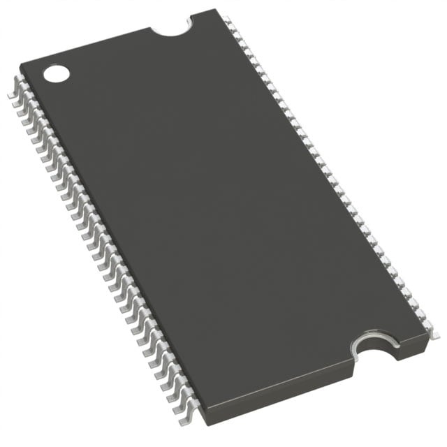
IC DRAM 512MBIT PAR 66TSOP |
|---|---|
| Quantity | 860 Available (as of June 18, 2026) |

| Product Category | DRAM Memory |
|---|---|
| Manufacturer | Micron Technology Inc. |
| Manufacturing Status | Obsolete |
| Manufacturer Standard Lead Time | Contact Us |
| Datasheet |
Specifications & Environmental
| Device Package | 66-TSOP | Memory Format | DRAM | Technology | SDRAM - DDR | ||
|---|---|---|---|---|---|---|---|
| Memory Size | 512 Mbit | Access Time | 700 ps | Grade | Industrial | ||
| Clock Frequency | 167 MHz | Voltage | 2.3V ~ 2.7V | Memory Type | Volatile | ||
| Operating Temperature | -40°C ~ 85°C (TA) | Write Cycle Time Word Page | 15 ns | Packaging | 66-TSSOP (0.400", 10.16mm Width) | ||
| Mounting Method | Volatile | Memory Interface | Parallel | Memory Organization | 64M x 8 | ||
| Moisture Sensitivity Level | 4 (72 Hours) | RoHS Compliance | RoHS non-compliant | REACH Compliance | REACH Unaffected | ||
| Qualification | N/A | ECCN | EAR99 | HTS Code | 8542.32.0024 |
Overview of MT46V64M8TG-6T IT:D TR – IC DRAM 512Mbit Parallel DDR SDRAM, 66-TSSOP
The MT46V64M8TG-6T IT:D TR is a 512 Mbit DDR SDRAM organized as 64M × 8 with a parallel memory interface in a 66‑pin TSSOP package. It implements a double-data-rate architecture with internal DLL and source-synchronous DQS to support two data accesses per clock cycle.
Designed for board‑level memory expansion where a compact 66‑TSSOP footprint, 2.3–2.7 V supply operation, and industrial temperature capability (−40 °C to +85 °C) are required, the device provides deterministic timing and programmable burst lengths for system memory buffering and working storage.
Key Features
- Core / Architecture Internal pipelined DDR architecture with two data transfers per clock and a DLL to align DQ/DQS transitions with the clock.
- Memory Organization 512 Mbit total capacity arranged as 64M × 8 with four internal banks, suitable for parallel DDR memory implementations.
- Data Strobe and Clocking Bidirectional data strobe (DQS) transmitted/received with data for source‑synchronous capture and differential clock inputs (CK and CK#).
- Programmable Burst and Mask Programmable burst lengths of 2, 4, or 8 and data mask (DM) for write data masking.
- Performance / Timing Specified for up to 167 MHz clock frequency (speed grade 6T), access time ~700 ps and write cycle time (word page) 15 ns; data‑out windows and DQS‑DQ skew are defined in the datasheet.
- Power VDD/VDDQ supply range 2.3 V to 2.7 V (typical +2.5 V ± tolerances listed in the datasheet).
- Package 66‑pin TSSOP (0.400", 10.16 mm width) in a longer‑lead TSOP option for improved board‑level reliability.
- Temperature Range Industrial operating temperature range: −40 °C to +85 °C (TA).
- Reliability / Refresh Supports auto refresh and self refresh options; refresh count 8K cycles as specified for the 64M × 8 configuration.
Typical Applications
- Board‑level DDR memory Provides on‑board working memory in designs that require a parallel DDR SDRAM in a compact 66‑TSSOP footprint.
- Industrial electronics Suited for equipment operating within −40 °C to +85 °C where a 512 Mbit DDR device is required for buffering or temporary storage.
- System memory buffering Useful for designs needing programmable burst transfers, source‑synchronous DQS capture, and deterministic access windows for data buffering.
Unique Advantages
- DDR double‑data‑rate transfers: Two data accesses per clock cycle increase effective throughput without requiring higher clock rates.
- Source‑synchronous DQS with DLL: DQS alignment and DLL support improve timing margin for read/write operations and predictable data capture.
- Industrial temperature support: Specified operation from −40 °C to +85 °C addresses applications requiring extended temperature operation.
- Compact TSOP package: 66‑TSSOP (10.16 mm width) provides a small board footprint while retaining robust lead length for reliability.
- Flexible timing and burst control: Programmable burst lengths (2, 4, 8) and defined timing grades (including 6T speed grade at 167 MHz) allow tailoring to system performance needs.
- Standard 2.5 V signaling: VDD/VDDQ operation in the 2.3–2.7 V range supports SSTL‑2 style I/O environments documented in the datasheet.
Why Choose IC DRAM 512MBIT PAR 66TSOP?
The MT46V64M8TG-6T IT:D TR delivers a compact, industry‑rated DDR SDRAM solution with clear timing definitions, programmable burst lengths, and source‑synchronous DQS/DLL support. Its 64M × 8 organization and 512 Mbit capacity make it suitable for designs that require parallel DDR memory in a 66‑pin TSSOP package.
This device is appropriate for engineers specifying deterministic memory timing, industrial temperature operation, and a small board footprint. The set of documented timing grades, refresh behavior, and electrical supply window provide the verifiable specifications needed for integration into board‑level memory subsystems.
Request a quote or submit an inquiry to discuss availability, pricing, and lead times for the MT46V64M8TG-6T IT:D TR.