MT46V64M8TG-5B IT:J
| Part Description |
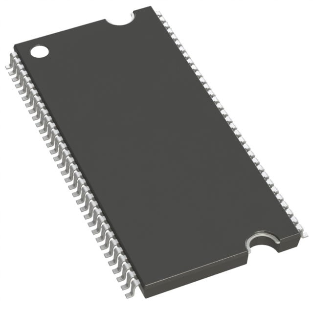
IC DRAM 512MBIT PARALLEL 66TSOP |
|---|---|
| Quantity | 853 Available (as of June 15, 2026) |

| Product Category | Memory |
|---|---|
| Manufacturer | Micron Technology Inc. |
| Manufacturing Status | Obsolete |
| Manufacturer Standard Lead Time | Contact Us |
| Datasheet |
Specifications & Environmental
| Device Package | 66-TSOP | Memory Format | DRAM | Technology | SDRAM - DDR | ||
|---|---|---|---|---|---|---|---|
| Memory Size | 512 Mbit | Access Time | 700 ps | Grade | Industrial | ||
| Clock Frequency | 200 MHz | Voltage | 2.5V ~ 2.7V | Memory Type | Volatile | ||
| Operating Temperature | -40°C ~ 85°C (TA) | Write Cycle Time Word Page | 15 ns | Packaging | 66-TSSOP (0.400", 10.16mm Width) | ||
| Mounting Method | Volatile | Memory Interface | Parallel | Memory Organization | 64M x 8 | ||
| Moisture Sensitivity Level | 3 (168 Hours) | RoHS Compliance | ROHS3 Compliant | REACH Compliance | REACH Unknown | ||
| Qualification | N/A | ECCN | EAR99 | HTS Code | 8542.32.0028 |
Overview of MT46V64M8TG-5B IT:J – IC DRAM 512MBIT PARALLEL 66TSOP
The MT46V64M8TG-5B IT:J is a 512 Mbit DDR SDRAM organized as 64M × 8 in a 66‑pin TSSOP package. It implements an internal pipelined double-data-rate architecture with differential clock inputs and source‑synchronous data strobe for read/write data capture.
Designed for systems that require parallel DDR memory with 2.5 V I/O and industrial temperature operation (–40 °C to +85 °C), the device provides programmable burst lengths, auto‑refresh and multiple timing grade options to match system performance requirements.
Key Features
- Core Architecture Internal, pipelined DDR architecture supporting two data accesses per clock cycle and four internal banks for concurrent operation.
- Memory Organization 512 Mbit capacity arranged as 64M × 8 with support for programmable burst lengths (2, 4, 8) and data mask (DM) for masked writes.
- Performance & Timing Speed grade -5B optimized for 5 ns cycle time (DDR400) with a listed clock frequency of 200 MHz and an access time of 700 ps; write cycle time (word page) is 15 ns.
- Interface & Timing Alignment Bidirectional data strobe (DQS) transmitted/received with data, DQS edge‑aligned for READs and center‑aligned for WRITEs, plus an internal DLL to align DQ/DQS with CK.
- Power & I/O 2.5 V I/O (SSTL_2 compatible); supply range noted as 2.5 V to 2.7 V and device-level VDD/VDDQ options documented in the datasheet.
- Refresh & Reliability Supports auto refresh and self refresh options (self refresh availability depends on device variant); 8K refresh cycle support specified in addressing tables.
- Package 66‑pin TSSOP (0.400", 10.16 mm width) package suitable for board‑level integration with a longer‑lead TSOP option noted for improved reliability.
- Operating Temperature Industrial temperature rating: –40 °C to +85 °C (TA).
Typical Applications
- Legacy and PC memory systems Compatible with speed‑grade categories listed for PC3200/PC2700/PC2100, making it applicable for designs targeting those DDR timing footprints.
- Industrial systems Industrial temperature range (–40 °C to +85 °C) supports deployment in control and instrumentation systems that require robust thermal tolerance.
- Embedded parallel DDR designs 64M × 8 organization and a parallel DDR interface enable use where compact, board‑mounted DDR memory is required.
Unique Advantages
- Double data‑rate throughput: Two data transfers per clock cycle provide higher data bandwidth within the same clock domain compared to single‑data‑rate memory.
- Source‑synchronous data capture: Bidirectional DQS timing and an internal DLL improve data alignment with the differential clock, easing system timing margins.
- Flexible timing options: Multiple speed grades (including -5B) and programmable burst lengths let designers balance latency and throughput for target applications.
- Industrial temperature capability: Rated for –40 °C to +85 °C operation to meet system requirements for harsher operating environments.
- Standard 2.5 V I/O: SSTL_2 compatible 2.5 V I/O simplifies integration with common DDR signaling standards used in parallel memory systems.
Why Choose IC DRAM 512MBIT PARALLEL 66TSOP?
The MT46V64M8TG-5B IT:J offers a compact 512 Mbit DDR SDRAM solution in a 66‑pin TSSOP package, combining DDR internal architecture, source‑synchronous DQS, and selectable timing grades to address system designs that require parallel DDR memory with defined timing and industrial temperature performance.
This device is well suited for engineers specifying board‑level DDR memory with 2.5 V I/O, 64M × 8 organization and the timing flexibility provided by programmable burst lengths and multiple speed grades. Its documented refresh and timing parameters support predictable system integration and validation.
Request a quote or submit a procurement inquiry to receive pricing and availability information for the MT46V64M8TG-5B IT:J.