
MT46V8M16P-75:D
| Part Description |
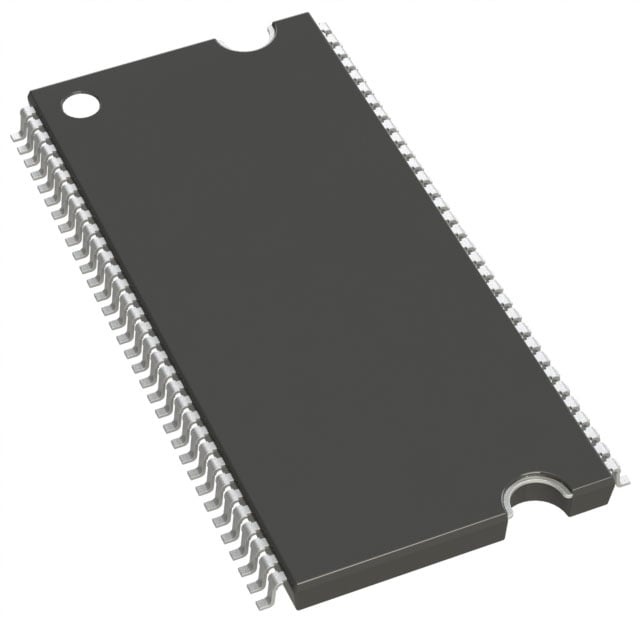
IC DRAM 128MBIT PAR 66TSOP |
|---|---|
| Quantity | 326 Available (as of June 14, 2026) |
| Product Category | Memory |
|---|---|
| Manufacturer | Micron Technology Inc. |
| Manufacturing Status | Obsolete |
| Manufacturer Standard Lead Time | Contact Us |
| Datasheet |
Specifications & Environmental
| Device Package | 66-TSOP | Memory Format | DRAM | Technology | SDRAM - DDR | ||
|---|---|---|---|---|---|---|---|
| Memory Size | 128 Mbit | Access Time | 750 ps | Grade | Commercial | ||
| Clock Frequency | 133 MHz | Voltage | 2.3V ~ 2.7V | Memory Type | Volatile | ||
| Operating Temperature | 0°C ~ 70°C (TA) | Write Cycle Time Word Page | 15 ns | Packaging | 66-TSSOP (0.400", 10.16mm Width) | ||
| Mounting Method | Volatile | Memory Interface | Parallel | Memory Organization | 8M x 16 | ||
| Moisture Sensitivity Level | 2 (1 Year) | RoHS Compliance | ROHS3 Compliant | REACH Compliance | REACH Unaffected | ||
| Qualification | N/A | ECCN | EAR99 | HTS Code | 8542.32.0002 |
Overview of MT46V8M16P-75:D – IC DRAM 128MBIT PAR 66TSOP
The MT46V8M16P-75:D is a 128 Mbit DDR SDRAM device organized as 8M × 16 with a parallel memory interface in a 66‑TSSOP package. It implements an internal, pipelined double-data-rate architecture with four internal banks, differential clock inputs, and source-synchronous data strobe (DQS).
Designed for systems that require a compact, board-mounted DDR memory device, the part operates at a clock frequency up to 133 MHz, supports programmable burst lengths, and targets designs needing 2.5 V I/O signaling and a commercial temperature range of 0 °C to 70 °C.
Key Features
- Core / Memory Architecture Double-data-rate (DDR) SDRAM with internal pipelined DDR architecture and four internal banks for concurrent operation. Device organization is 8M × 16 (128 Mbit).
- Performance & Timing Supports a clock frequency up to 133 MHz and an access time of 750 ps; write cycle time (word/page) is 15 ns. Programmable burst lengths of 2, 4, or 8 are supported.
- Data Capture & I/O Bidirectional data strobe (DQS) transmitted/received with data for source‑synchronous capture; the x16 configuration provides two DQS signals (one per byte). Data mask (DM) is supported (x16 has two DMs).
- Clock & Control Differential clock inputs (CK/CK#) with commands entered on positive CK edges and a DLL to align DQ/DQS with CK.
- Power & Voltage Supply voltage range specified at 2.3 V to 2.7 V (VDD / VDDQ per part specifications), with 2.5 V I/O (SSTL_2 compatible as specified in the datasheet).
- Package & Thermal 66‑TSSOP (0.400", 10.16 mm width) package with longer lead TSOP option (OCPL) noted for improved reliability. Operating temperature range: 0 °C to 70 °C (TA).
- Memory Interface & Reliability Parallel memory interface with auto refresh and self refresh modes and concurrent auto precharge option supported.
- Standards & Compatibility Speed-grade and PC interface compatibility entries are provided in the datasheet (examples include PC3200 / PC2700 / PC2100 speed-grade compatibility per device marking and timing tables).
Typical Applications
- Board-mounted DDR memory Use as on‑board 128 Mbit x16 DDR SDRAM where a 66‑TSSOP footprint is required.
- DDR memory subsystems Integration into memory subsystems that require programmable burst lengths, source‑synchronous DQS capture, and differential clock inputs.
- Systems targeting 133 MHz operation Designs that operate at or around a 133 MHz clock rate and leverage DDR double-data-rate transfers.
Unique Advantages
- Double-data-rate throughput: Internal pipelined DDR architecture provides two data accesses per clock cycle to increase effective bandwidth at the specified clock rates.
- Byte-level data control: DQS and DM signals (two per x16 device) enable source‑synchronous capture and write data masking on a per‑byte basis.
- Flexible timing options: Programmable burst lengths and documented speed‑grade timing tables allow matching of timing behavior to system requirements.
- Compact, board-ready package: 66‑TSSOP package (0.400", 10.16 mm width) provides a small footprint for space-constrained PCBs while offering longer lead TSOP (OCPL) for improved reliability.
- Voltage range for DDR I/O: Specified VDD/VDDQ range of 2.3 V to 2.7 V with 2.5 V I/O (SSTL_2 compatibility) supports standard DDR signaling environments.
Why Choose IC DRAM 128MBIT PAR 66TSOP?
The MT46V8M16P-75:D delivers a compact, board-mounted DDR SDRAM option with 128 Mbit density in an 8M × 16 organization, suitable for designs that require DDR operation at up to 133 MHz and source-synchronous data capture. Its combination of programmable burst lengths, DQS/DM support, and documented speed‑grade compatibility provides predictable timing behavior for system integration.
This device is well suited to engineers specifying on‑board DDR memory in a 66‑TSSOP footprint where commercial temperature operation (0 °C to 70 °C), a 2.3 V–2.7 V supply range, and standard DDR signaling are required. Datasheet timing tables and configuration options support engineering evaluation and system-level timing alignment.
Request a quote or submit a quote to obtain pricing and availability for MT46V8M16P-75:D.


