MT47H128M4B6-25:D TR
| Part Description |
IC DRAM 512MBIT PARALLEL 60FBGA |
|---|---|
| Quantity | 169 Available (as of June 15, 2026) |

| Product Category | Memory |
|---|---|
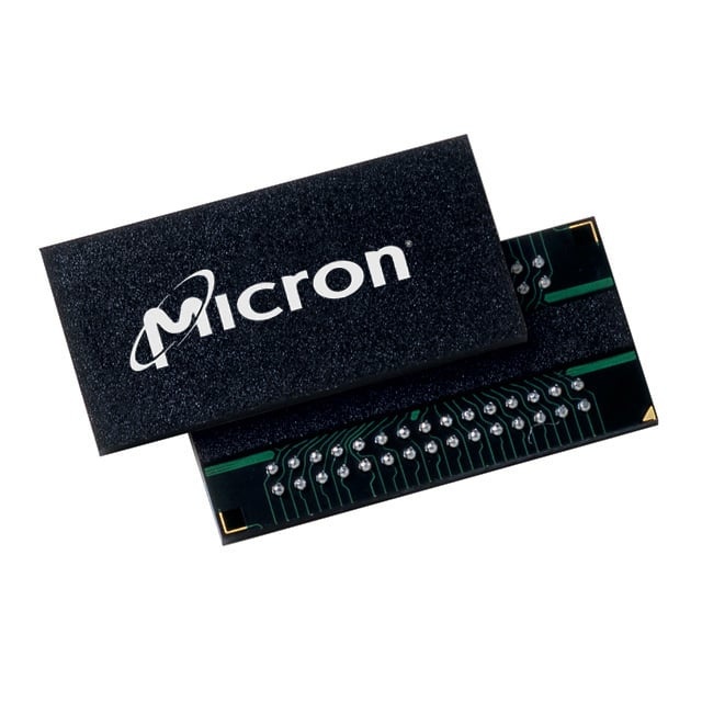
| Manufacturer | Micron Technology Inc. |
| Manufacturing Status | Obsolete |
| Manufacturer Standard Lead Time | Contact Us |
| Datasheet |
Specifications & Environmental
| Device Package | 60-FBGA | Memory Format | DRAM | Technology | SDRAM - DDR2 | ||
|---|---|---|---|---|---|---|---|
| Memory Size | 512 Mbit | Access Time | 400 ps | Grade | Commercial (Extended) | ||
| Clock Frequency | 400 MHz | Voltage | 1.7V ~ 1.9V | Memory Type | Volatile | ||
| Operating Temperature | 0°C ~ 85°C (TC) | Write Cycle Time Word Page | 15 ns | Packaging | 60-FBGA | ||
| Mounting Method | Volatile | Memory Interface | Parallel | Memory Organization | 128M x 4 | ||
| Moisture Sensitivity Level | 3 (168 Hours) | RoHS Compliance | ROHS Compliant | REACH Compliance | REACH Unaffected | ||
| Qualification | N/A | ECCN | 3A991B2A | HTS Code | 8542.32.0024 |
Overview of MT47H128M4B6-25:D TR – 512Mbit DDR2 SDRAM, 60‑FBGA
The MT47H128M4B6-25:D TR is a 512 Mbit DDR2 SDRAM organized as 128M x 4 with a parallel memory interface in a 60-ball FBGA package. It implements a 4n-bit prefetch architecture with 4 internal banks and supports standard DDR2 timing and signaling for systems operating at a 1.8 V nominal supply.
This device is targeted at commercial temperature applications and offers programmable timing, selectable burst lengths and on-die features intended for system designs that require compact, low‑voltage DDR2 memory in a 60‑FBGA footprint.
Key Features
- Memory Core & Organization 512 Mbit density organized as 128M x 4 with 4 internal banks and a 4n‑bit prefetch architecture for standard DDR2 operation.
- Performance & Timing Supports DDR2 data rates up to 400 MT/s (clock frequency noted as 400 MHz), programmable CAS latency, selectable burst lengths (BL = 4 or 8) and timing grades including the -25 speed grade for DDR2‑800 operation as documented in the datasheet.
- Signal Integrity On‑die termination (ODT) and an internal DLL align DQ/DQS transitions with CK; differential data strobe (DQS/DQS#) options are available to support high‑speed data capture.
- Voltage & I/O Nominal VDD/VDDQ = 1.8 V (specified VDD = +1.8V ±0.1V; product supply range 1.7 V – 1.9 V) with JEDEC‑standard 1.8 V I/O (SSTL_18‑compatible).
- Package 60‑ball FBGA package case suited for board‑level integration where a compact BGA footprint is required.
- Operating Range Commercial temperature range: 0 °C to 85 °C (T_C) as specified for this part number.
- Refresh & Reliability Standard DDR2 refresh architecture (8,192‑cycle refresh) and supported timing features including posted CAS additive latency and WRITE/READ relationship (WRITE latency = READ latency − 1 tCK).
- Compliance & Options Datasheet indicates RoHS compliance and multiple package and timing options; FBGA packaging is available in Pb‑free and leaded variants per datasheet option listings.
Typical Applications
- Commercial embedded systems Parallel DDR2 memory for systems that require 512 Mbit density and a commercial operating temperature range (0 °C to 85 °C).
- Compact board‑level memory expansion 60‑FBGA package provides a compact footprint for designs that need high‑density DDR2 memory in a small BGA package.
- Systems using 1.8 V DDR2 I/O Suitable for platforms designed around JEDEC‑standard 1.8 V signaling and SSTL_18 compatibility.
Unique Advantages
- High‑density 512 Mbit in a small package: 128M x 4 organization delivers 512 Mbit capacity in a 60‑ball FBGA for space‑constrained boards.
- Low‑voltage DDR2 operation: 1.8 V nominal supply (1.7 V–1.9 V range) reduces power compared with higher‑voltage memories while maintaining DDR2 signaling standards.
- Flexible timing and bursting: Programmable CAS latency and selectable burst lengths (4 or 8) allow designers to tune throughput and latency for system requirements.
- Built‑in signal integrity features: On‑die termination and an internal DLL improve data capture margins and simplify board‑level termination strategies.
- Vendor traceability and documented options: Multiple speed grades, package revisions and options are listed in the manufacturer datasheet for design selection and comparability.
Why Choose MT47H128M4B6-25:D TR?
The MT47H128M4B6-25:D TR positions itself as a compact, low‑voltage DDR2 SDRAM option delivering 512 Mbit density with standard JEDEC 1.8 V I/O, on‑die termination and flexible timing features. Its 60‑FBGA footprint and commercial temperature rating make it appropriate for board‑level memory expansion in systems that require DDR2 performance within a compact package.
This part is suited to designers who need verifiable DDR2 behavior—programmable CAS, selectable burst lengths, DLL alignment and documented timing grades—backed by manufacturer datasheet specifications for selection and integration into commercial temperature‑range products.
Request a quote or submit an inquiry to receive pricing and availability information for MT47H128M4B6-25:D TR.