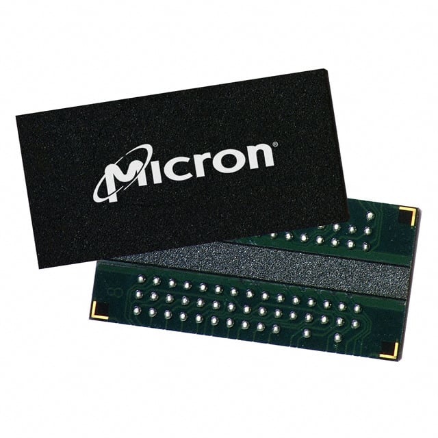
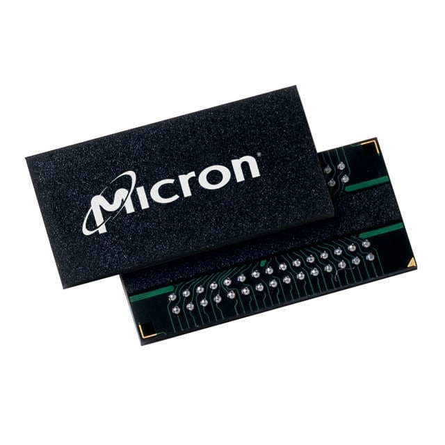
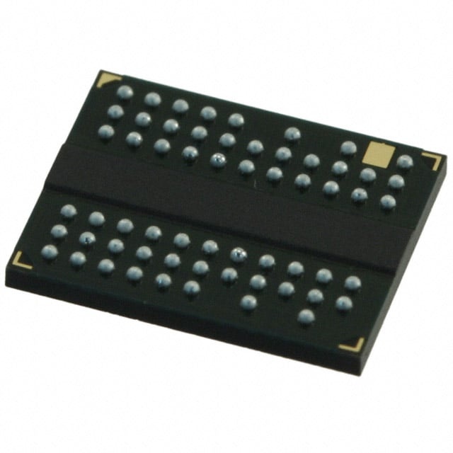
MT47H128M4CF-25E:G
| Part Description |
IC DRAM 512MBIT PARALLEL 60FBGA |
|---|---|
| Quantity | 249 Available (as of June 15, 2026) |
| Product Category | Memory |
|---|---|
| Manufacturer | Micron Technology Inc. |
| Manufacturing Status | Obsolete |
| Manufacturer Standard Lead Time | Contact Us |
| Datasheet |
Specifications & Environmental
| Device Package | 60-FBGA (8x10) | Memory Format | DRAM | Technology | SDRAM - DDR2 | ||
|---|---|---|---|---|---|---|---|
| Memory Size | 512 Mbit | Access Time | 400 ps | Grade | Commercial (Extended) | ||
| Clock Frequency | 400 MHz | Voltage | 1.7V ~ 1.9V | Memory Type | Volatile | ||
| Operating Temperature | 0°C ~ 85°C (TC) | Write Cycle Time Word Page | 15 ns | Packaging | 60-TFBGA | ||
| Mounting Method | Volatile | Memory Interface | Parallel | Memory Organization | 128M x 4 | ||
| Moisture Sensitivity Level | 3 (168 Hours) | RoHS Compliance | ROHS3 Compliant | REACH Compliance | REACH Unaffected | ||
| Qualification | N/A | ECCN | EAR99 | HTS Code | 8542.32.0028 |
Overview of MT47H128M4CF-25E:G – IC DRAM 512MBIT PARALLEL 60FBGA
The MT47H128M4CF-25E:G is a 512 Mbit DDR2 SDRAM organized as 128M × 4 with a parallel memory interface in a 60-ball TFBGA (8 × 10 mm) package. It is a volatile, JEDEC-compatible DDR2 device designed for systems requiring compact, low-voltage synchronous DRAM.
Key architectural elements include a 4n‑bit prefetch, four internal banks and programmable CAS latency; the device targets applications that need configurable DDR2 bandwidth and compact board-level integration while operating from a 1.7 V to 1.9 V supply over a commercial temperature range.
Key Features
- Memory Core 512 Mbit DDR2 SDRAM organized as 128M × 4 with four internal banks for concurrent operation.
- DDR2 Architecture 4n‑bit prefetch architecture, DLL to align DQ and DQS with CK, and programmable CAS latency with posted CAS additive latency options.
- Timing Options Supports JEDEC timing grades; the part number variant includes the -25E timing option (2.5 ns @ CL = 5, DDR2‑800) and the datasheet lists multiple speed/timing grades for selection.
- Interface and Signaling JEDEC‑standard 1.8 V I/O (SSTL_18‑compatible) with differential data strobe (DQS/DQS#) options and optional duplicate output strobe (RDQS) for x8 configurations.
- Power and Voltage Single‑supply operation with specified VDD range of 1.7 V to 1.9 V (datasheet nominal VDD = 1.8 V ± 0.1 V) and adjustable data‑output drive strength.
- Data Integrity and Performance On‑die termination (ODT) option and DLL support for improved signal timing and integrity; selectable burst lengths of 4 or 8 to match transfer patterns.
- Refresh and Reliability 8192‑cycle refresh with a 64 ms refresh interval as specified in the datasheet.
- Package and Temperature 60‑ball TFBGA (8 mm × 10 mm) package; commercial operating temperature range 0°C to 85°C.
- Standards and Compliance JEDEC DDR2 architecture with RoHS‑compliant designation indicated in the datasheet.
Unique Advantages
- High memory density in a compact package: 512 Mbit capacity in a 60‑ball FBGA (8 × 10 mm) for space‑constrained designs.
- Flexible performance tuning: Programmable CAS latency, posted CAS additive latency and selectable burst lengths allow designers to match timing to system requirements.
- Low‑voltage operation: VDD range of 1.7 V–1.9 V and SSTL_18‑compatible I/O reduce system power and simplify interface design with 1.8 V signaling.
- Improved signal integrity: On‑die termination (ODT) and a DLL to align DQ/DQS transitions with CK help maintain reliable high‑speed transfers.
- Concurrency and throughput: Four internal banks and 4n‑bit prefetch architecture enable overlapping operations for sustained data throughput.
- JEDEC DDR2 timing options: Multiple speed/timing grades (including the -25E option) provide choices for performance/cost tradeoffs.
Why Choose IC DRAM 512MBIT PARALLEL 60FBGA?
The MT47H128M4CF-25E:G positions itself as a configurable DDR2 memory building block for systems that require 512 Mbit density in a compact FBGA footprint. Its programmable timing, ODT, DLL and low‑voltage 1.8 V signaling allow designers to tailor memory behavior to platform timing and power targets while maintaining JEDEC DDR2 architecture.
This device is suitable for designs needing a parallel DDR2 SDRAM solution with commercial temperature support and a small board footprint; the combination of internal banks, selectable burst lengths and adjustable drive strength offers practical levers for balancing throughput, signal integrity and power.
Request a quote or submit an inquiry to receive pricing, availability and additional technical support for MT47H128M4CF-25E:G.