MT47H16M16BG-3 IT:B TR
| Part Description |
IC DRAM 256MBIT PARALLEL 84FBGA |
|---|---|
| Quantity | 2,000 Available (as of June 9, 2026) |

| Product Category | Memory |
|---|---|
| Manufacturer | Micron Technology Inc. |
| Manufacturing Status | Obsolete |
| Manufacturer Standard Lead Time | Contact Us |
| Datasheet |
Specifications & Environmental
| Device Package | 84-FBGA (8x14) | Memory Format | DRAM | Technology | SDRAM - DDR2 | ||
|---|---|---|---|---|---|---|---|
| Memory Size | 256 Mbit | Access Time | 450 ps | Grade | Automotive | ||
| Clock Frequency | 333 MHz | Voltage | 1.7V ~ 1.9V | Memory Type | Volatile | ||
| Operating Temperature | -40°C ~ 95°C (TC) | Write Cycle Time Word Page | 15 ns | Packaging | 84-FBGA | ||
| Mounting Method | Volatile | Memory Interface | Parallel | Memory Organization | 16M x 16 | ||
| Moisture Sensitivity Level | 3 (168 Hours) | RoHS Compliance | ROHS Compliant | REACH Compliance | REACH Unaffected | ||
| Qualification | N/A | ECCN | 3A991B2A | HTS Code | 8542.32.0024 |
Overview of MT47H16M16BG-3 IT:B TR – IC DRAM 256MBIT PARALLEL 84FBGA
The MT47H16M16BG-3 IT:B TR is a 256 Mbit DDR2 SDRAM organized as 16M × 16 with a parallel memory interface in an 84-ball FBGA (8 × 14) package. It implements DDR2 SDRAM architecture and is offered with industrial temperature capability for applications requiring extended operating temperature range.
This device targets systems requiring compact, low-voltage DDR2 memory with programmable timing and on-die signal integrity features. Key value comes from its DDR2 architecture, industrial temperature rating, and compact FBGA mounting.
Key Features
- Memory Architecture DDR2 SDRAM organized as 16M × 16 for a total of 256 Mbit; 4 internal banks for concurrent operation.
- Performance Clock frequency specified at 333 MHz with an access time of 450 ps and a word/page write cycle time of 15 ns.
- Voltage and I/O Operates from 1.7 V to 1.9 V; datasheet specifies VDD and VDDQ = +1.8 V ±0.1 V with JEDEC-standard 1.8 V I/O (SSTL_18-compatible).
- Timing and Burst Control Programmable CAS latency and selectable burst lengths (BL = 4 or 8) to tune latency and throughput per system requirements.
- Signal Integrity DLL to align DQ and DQS transitions with CK and on-die termination (ODT) to improve signal margins; supports JEDEC clock jitter specification.
- Refresh and Reliability 64 ms, 8,192-cycle refresh and four internal banks to support sustained memory operation.
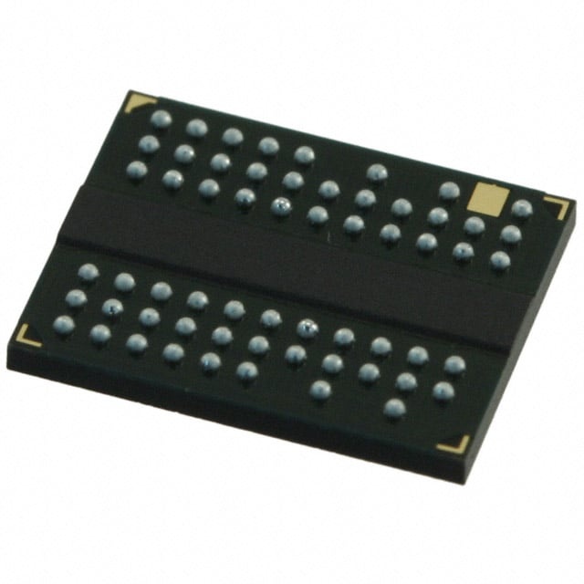
- Package & Mounting 84-ball FBGA (8 mm × 14 mm) package, intended for surface-mount assembly in compact designs.
- Temperature Range Industrial temperature option with an operating temperature range of -40°C to 95°C (TC).
- Additional Functional Options Differential data strobe (DQS/DQS#) option, duplicate output strobe (RDQS) option for x8 devices, adjustable data-output drive strength.
- Compliance Datasheet lists RoHS compliance for offered device options.
Typical Applications
- Industrial and Embedded Systems Industrial temperature rating and compact FBGA packaging make the device suitable for embedded controllers and industrial electronics that require DDR2 memory in constrained board space.
- Board-Level Memory Subsystems Used as parallel DDR2 DRAM in memory subsystems where 256 Mbit density and x16 organization are required.
- Compact Consumer or Communication Modules Small FBGA footprint and low-voltage operation support integration into space-constrained consumer and communication modules that use DDR2 memory.
Unique Advantages
- Industrial Temperature Capability: Designed for -40°C to 95°C (TC), enabling deployment in systems exposed to extended temperature ranges.
- Low-Voltage DDR2 Operation: 1.7 V–1.9 V supply range (VDD and VDDQ = 1.8 V ±0.1 V) reduces power domain requirements in modern system designs.
- Programmable Timing Flexibility: Programmable CAS latency and selectable burst lengths allow designers to balance latency and throughput per application needs.
- Signal Integrity Features: DLL alignment and on-die termination improve data timing and reduce external termination complexity.
- Compact FBGA Packaging: 84-ball FBGA (8 × 14 mm) provides high-density mounting for compact boards while maintaining x16 data width.
- Standardized JEDEC Support: JEDEC-compatible I/O and clock jitter support simplifies integration with standard DDR2 controllers and memory subsystems.
Why Choose MT47H16M16BG-3 IT:B TR?
The MT47H16M16BG-3 IT:B TR positions itself as a compact DDR2 SDRAM solution that combines 256 Mbit density, low-voltage operation, and industrial temperature capability in an 84-ball FBGA package. Its programmable timing, on-die termination, and DLL provide the timing and signal-integrity controls needed for reliable board-level memory implementations.
This device is well suited to designers building industrial, embedded, or compact memory subsystems that require a verified DDR2 architecture, x16 organization, and temperature robustness. The combination of performance-focused timing options and a small FBGA footprint supports scalable, reliable system designs with clear integration parameters.
Request a quote or submit an RFQ to check availability, lead times, and pricing for the MT47H16M16BG-3 IT:B TR.