MT47H16M16BG-5E:B
| Part Description |
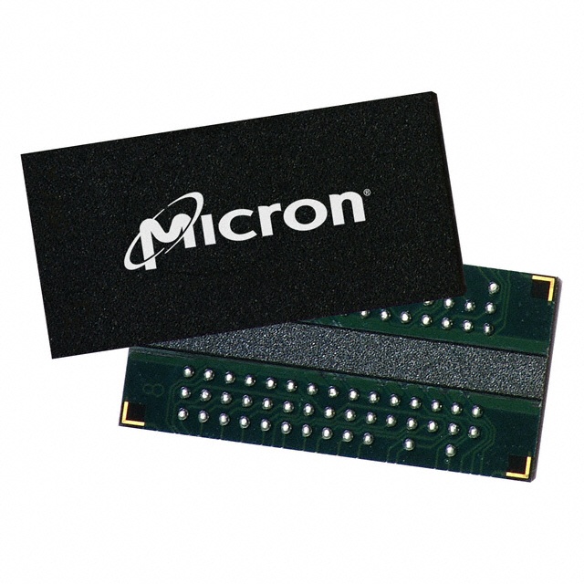
IC DRAM 256MBIT PARALLEL 84FBGA |
|---|---|
| Quantity | 964 Available (as of June 18, 2026) |

| Product Category | DRAM Memory |
|---|---|
| Manufacturer | Micron Technology Inc. |
| Manufacturing Status | Obsolete |
| Manufacturer Standard Lead Time | Contact Us |
| Datasheet |
Specifications & Environmental
| Device Package | 84-FBGA (8x14) | Memory Format | DRAM | Technology | SDRAM - DDR2 | ||
|---|---|---|---|---|---|---|---|
| Memory Size | 256 Mbit | Access Time | 600 ps | Grade | Commercial (Extended) | ||
| Clock Frequency | 200 MHz | Voltage | 1.7V ~ 1.9V | Memory Type | Volatile | ||
| Operating Temperature | 0°C ~ 85°C (TC) | Write Cycle Time Word Page | 15 ns | Packaging | 84-FBGA | ||
| Mounting Method | Volatile | Memory Interface | Parallel | Memory Organization | 16M x 16 | ||
| Moisture Sensitivity Level | 2 (1 Year) | RoHS Compliance | ROHS3 Compliant | REACH Compliance | REACH Unaffected | ||
| Qualification | N/A | ECCN | EAR99 | HTS Code | 8542.32.0024 |
Overview of MT47H16M16BG-5E:B – IC DRAM 256MBIT PARALLEL 84FBGA
The MT47H16M16BG-5E:B is a 256 Mbit DDR2 SDRAM organized as 16M x 16 with a parallel memory interface in an 84-ball FBGA package. It implements DDR2 architecture features such as a 4n-bit prefetch and an internal DLL to align data transitions with clock signals.
Designed for DDR2-compatible memory subsystems, this device provides a compact 84-FBGA form factor, 1.7–1.9 V supply operation, and timing options suited to 200 MHz clock operation (400 MT/s data rate), making it appropriate for applications requiring mid-density volatile system memory.
Key Features
- Core architecture 4n-bit prefetch DDR2 SDRAM with an internal DLL and four internal banks for concurrent operation.
- Memory capacity & organization 256 Mbit total capacity, organized as 16M × 16 with 4 internal banks; JEDEC address mapping provided in datasheet.
- Interface & timing Parallel DDR2 interface with programmable CAS latency, selectable burst lengths (BL = 4 or 8), and support for JEDEC clock jitter specifications. Specified clock frequency: 200 MHz; access time: 600 ps; write cycle time (word page): 15 ns.
- Voltage & I/O VDD and VDDQ nominally +1.8 V (range 1.7 V to 1.9 V); JEDEC-standard 1.8 V I/O (SSTL_18-compatible).
- Signal options Differential data strobe (DQS/DQS#) available as an option; DLL aligns DQ and DQS transitions with CK.
- Data integrity & control On-die termination (ODT) and adjustable data-output drive strength are supported; refresh architecture includes 64 ms / 8,192-cycle refresh.
- Package 84-ball FBGA (8 mm × 14 mm) compact package in an FBGA footprint for high-density board designs.
- Temperature range Commercial operating temperature range: 0 °C to 85 °C (T_C), per the specified operating temperature.
- Standards & compliance Device documentation lists RoHS compliance as a feature in the product datasheet.
Typical Applications
- DDR2 system memory Use as volatile system memory in DDR2-compatible designs requiring a 256 Mbit x16 device.
- Compact module integration Suitable for board-level designs that require a small 84-ball FBGA footprint for mid-density DRAM.
- Parallel-interface buffering Employed where parallel DDR2 buffering with programmable latency and selectable burst lengths is needed.
Unique Advantages
- Mid-density 16M × 16 organization: Provides 256 Mbit capacity in a x16 configuration that simplifies data-path implementation for parallel memory systems.
- Low-voltage DDR2 operation: Nominal 1.8 V operation (1.7–1.9 V range) reduces power domain complexity where 1.8 V supplies are used.
- Compact FBGA packaging: 84-ball FBGA (8×14 mm) minimizes board area while maintaining ball-out connectivity for high-density layouts.
- Flexible timing and drive options: Programmable CAS latency, selectable burst lengths, adjustable output drive strength and ODT enable tuning for system timing and signal integrity.
- DDR2 feature set: Internal DLL, differential DQS option, and 4-bank architecture support common DDR2 timing and performance requirements.
Why Choose MT47H16M16BG-5E:B?
The MT47H16M16BG-5E:B positions itself as a compact, mid-density DDR2 SDRAM device for designs that require a 256 Mbit x16 memory element with standard DDR2 features. Its 84-FBGA package, 1.7–1.9 V supply range, and programmable timing options make it suitable for DDR2-compatible memory subsystems where board area, voltage compatibility, and timing flexibility matter.
This device is appropriate for engineers specifying volatile DRAM capacity in embedded and board-level systems that adhere to DDR2 signaling and JEDEC timing conventions, and where commercial temperature operation (0 °C to 85 °C) is acceptable.
Request a quote or submit an inquiry to obtain current pricing and availability for the MT47H16M16BG-5E:B DRAM device.