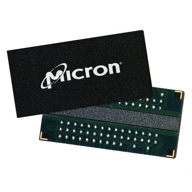
MT47H32M16BN-5E:D TR
| Part Description |
IC DRAM 512MBIT PARALLEL 84FBGA |
|---|---|
| Quantity | 1,584 Available (as of June 15, 2026) |

| Product Category | Memory |
|---|---|
| Manufacturer | Micron Technology Inc. |
| Manufacturing Status | Obsolete |
| Manufacturer Standard Lead Time | Contact Us |
| Datasheet |
Specifications & Environmental
| Device Package | 84-FBGA (10x12.5) | Memory Format | DRAM | Technology | SDRAM - DDR2 | ||
|---|---|---|---|---|---|---|---|
| Memory Size | 512 Mbit | Access Time | 600 ps | Grade | Commercial (Extended) | ||
| Clock Frequency | 200 MHz | Voltage | 1.7V ~ 1.9V | Memory Type | Volatile | ||
| Operating Temperature | 0°C ~ 85°C (TC) | Write Cycle Time Word Page | 15 ns | Packaging | 84-TFBGA | ||
| Mounting Method | Volatile | Memory Interface | Parallel | Memory Organization | 32M x 16 | ||
| Moisture Sensitivity Level | 3 (168 Hours) | RoHS Compliance | ROHS3 Compliant | REACH Compliance | REACH Unaffected | ||
| Qualification | N/A | ECCN | EAR99 | HTS Code | 8542.32.0024 |
Overview of MT47H32M16BN-5E:D TR – IC DRAM 512MBIT PARALLEL 84FBGA
The MT47H32M16BN-5E:D TR is a 512 Mbit DDR2 SDRAM device organized as 32M × 16 with a parallel memory interface in an 84-ball FBGA package. It implements DDR2 architecture with 4 internal banks and JEDEC‑standard 1.8 V I/O signaling for synchronous high-speed memory use.
This device is intended for commercial-temperature systems requiring low-voltage DDR2 memory with selectable latency and burst lengths, providing a compact 84‑FBGA footprint for space-constrained board designs.
Key Features
- Core / Architecture DDR2 SDRAM core with 4 internal banks and a 4n‑bit prefetch architecture for standard DDR2 operation.
- Memory Organization 512 Mbit capacity configured as 32M × 16, supporting parallel data transfers.
- Performance / Timing Supports a clock frequency up to 200 MHz with an access time of 600 ps and a write cycle time (word page) of 15 ns. Programmable CAS latency and selectable burst lengths (4 or 8) are supported.
- Power / I/O Low‑voltage operation with VDD/VDDQ = 1.7 V to 1.9 V (JEDEC‑standard 1.8 V I/O). On‑die termination (ODT) and adjustable data‑output drive strength are available.
- Interface Parallel memory interface with differential data strobe (DQS/DQS#) options and DLL to align DQ/DQS transitions with CK.
- Reliability / Refresh 4 internal banks for concurrent operation and a 64 ms, 8,192‑cycle refresh scheme.
- Package 84‑ball FBGA (supplier package: 84‑FBGA 10 mm × 12.5 mm) compact package suitable for high‑density layouts.
- Temperature Range Commercial operating temperature: 0 °C to 85 °C (T_C).
- Compliance Datasheet indicates RoHS compliance.
Typical Applications
- Embedded memory subsystems For designs that require a 512 Mbit DDR2 parallel memory device with a compact 84‑FBGA footprint.
- Consumer and commercial electronics Use in commercial‑temperature boards where low‑voltage 1.8 V DDR2 memory and standard JEDEC I/O are required.
- Space‑constrained PCB designs Compact 84‑ball FBGA package supports high-density board layouts and module integration.
Unique Advantages
- Low‑voltage DDR2 operation: VDD/VDDQ range of 1.7 V–1.9 V reduces power draw compared with higher‑voltage memories while maintaining DDR2 signaling.
- Flexible timing and burst control: Programmable CAS latency and selectable burst lengths (4 or 8) allow tuning for system timing and throughput requirements.
- On‑die termination and drive control: ODT and adjustable data‑output drive strength simplify signal integrity management on high‑speed boards.
- Compact FBGA footprint: 84‑ball FBGA (10 mm × 12.5 mm) enables dense board integration without sacrificing memory capacity.
- JEDEC‑standard I/O compatibility: 1.8 V I/O (SSTL_18‑compatible) ensures predictable interfacing with standard DDR2 memory controllers.
- Established vendor backing: Device is documented in Micron’s DDR2 SDRAM family datasheet for traceable specifications and system integration details.
Why Choose MT47H32M16BN-5E:D TR?
The MT47H32M16BN-5E:D TR positions itself as a commercial‑temperature DDR2 SDRAM solution offering a 512 Mbit density in a 32M × 16 organization, combining low‑voltage 1.8 V operation with programmable timing options and on‑die termination. Its 84‑FBGA package and parallel interface make it suitable for compact, high‑density memory subsystems where JEDEC‑standard DDR2 signaling is required.
This device is appropriate for engineers and procurement teams specifying DDR2 memory for commercial systems that need verified timing control, selectable burst modes, and a small package size backed by Micron’s device documentation.
Request a quote or submit an inquiry to check availability, lead times and pricing for MT47H32M16BN-5E:D TR.