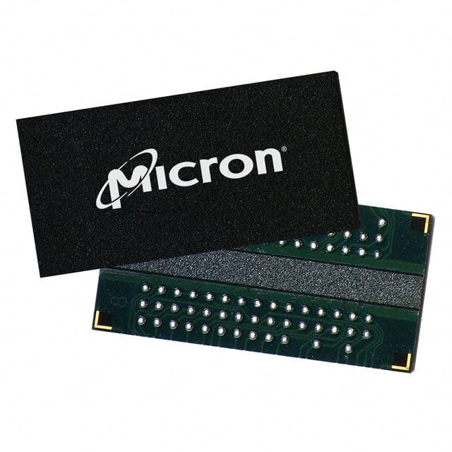
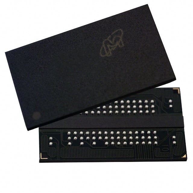
MT47H32M16BN-5E IT:D TR
| Part Description |
IC DRAM 512MBIT PARALLEL 84FBGA |
|---|---|
| Quantity | 47 Available (as of June 15, 2026) |

| Product Category | Memory |
|---|---|
| Manufacturer | Micron Technology Inc. |
| Manufacturing Status | Obsolete |
| Manufacturer Standard Lead Time | Contact Us |
| Datasheet |
Specifications & Environmental
| Device Package | 84-FBGA (10x12.5) | Memory Format | DRAM | Technology | SDRAM - DDR2 | ||
|---|---|---|---|---|---|---|---|
| Memory Size | 512 Mbit | Access Time | 600 ps | Grade | Automotive | ||
| Clock Frequency | 200 MHz | Voltage | 1.7V ~ 1.9V | Memory Type | Volatile | ||
| Operating Temperature | -40°C ~ 95°C (TC) | Write Cycle Time Word Page | 15 ns | Packaging | 84-TFBGA | ||
| Mounting Method | Volatile | Memory Interface | Parallel | Memory Organization | 32M x 16 | ||
| Moisture Sensitivity Level | 3 (168 Hours) | RoHS Compliance | ROHS3 Compliant | REACH Compliance | REACH Unaffected | ||
| Qualification | N/A | ECCN | 3A991B2A | HTS Code | 8542.32.0024 |
Overview of MT47H32M16BN-5E IT:D TR – IC DRAM 512MBIT PARALLEL 84FBGA
The MT47H32M16BN-5E IT:D TR is a 512Mbit DDR2 SDRAM organized as 32M x 16 with a parallel memory interface in an 84-ball FBGA package. It implements DDR2 architecture with a 4n-bit prefetch and internal features such as a DLL, on-die termination and selectable burst lengths to support synchronous high-speed memory operation.
This device targets board-level memory subsystems and embedded designs that require a 512Mbit DDR2 DRAM with industrial-temperature operation and low-voltage (1.7–1.9 V) supply rails.
Key Features
- Core / Memory Architecture 512Mbit DDR2 SDRAM organized as 32M × 16 with 4 internal banks and a 4n-bit prefetch architecture for DDR2 operation.
- Performance & Timing Supports programmable CAS latency, posted CAS additive latency, selectable burst lengths (4 or 8) and a DLL to align DQ and DQS with CK; specified access time 600 ps and clock frequency 200 MHz.
- Interface JEDEC-standard 1.8 V I/O (SSTL_18-compatible) with optional differential data strobe (DQS/DQS#) and duplicate output strobe (RDQS) option for x8 devices.
- Power Low-voltage operation with VDD / VDDQ = 1.8 V ±0.1 V (spec sheet range 1.7 V–1.9 V) to support reduced-power system designs.
- System Reliability & Timing Controls On-die termination (ODT), adjustable data-output drive strength, and a 64 ms, 8,192-cycle refresh scheme to maintain signal integrity and data retention.
- Package & Temperature Options 84-ball FBGA package (10 mm × 12.5 mm footprint option shown) and an Industrial temperature option rated for –40°C to 95°C (TC).
- Standards & Options RoHS compliant with options for various FBGA revisions and timing grades; supports JEDEC clock jitter specification.
Typical Applications
- Industrial Systems Used in control and instrumentation platforms that require DDR2 memory capable of industrial temperature operation (–40°C to 95°C TC).
- Board-level Memory Subsystems Deployed on memory modules and daughtercards where a 512Mbit x16 DDR2 device in an 84-ball FBGA footprint is required.
- Embedded Designs Suitable for embedded devices and appliances that integrate parallel DDR2 SDRAM for system working memory with programmable timing.
Unique Advantages
- Industrial-temperature rating: Rated for –40°C to 95°C (TC), enabling designs that require extended temperature operation.
- Low-voltage DDR2 operation: VDD/VDDQ = 1.8 V ±0.1 V (1.7–1.9 V range) reduces system power compared with higher-voltage memory solutions.
- Flexible timing and latency control: Programmable CAS latency, posted CAS additive latency, selectable burst lengths and DLL alignment allow designers to tune performance to system timing requirements.
- Signal integrity features: On-die termination and adjustable drive strength help manage signal integrity in high-speed parallel memory interfaces.
- Compact FBGA footprint: 84-ball FBGA package (example 10 mm × 12.5 mm option) provides a compact, board-friendly package for dense designs.
- JEDEC-compliant I/O: SSTL_18-compatible 1.8 V I/O and support for JEDEC clock jitter specifications simplify system-level compliance.
Why Choose MT47H32M16BN-5E IT:D TR?
The MT47H32M16BN-5E IT:D TR combines DDR2 architecture with configurable timing, on-die termination and industrial-temperature capability to deliver a stable 512Mbit DRAM option for board-level and embedded memory designs. Its low-voltage operation and FBGA packaging make it suitable for compact systems that require a parallel DDR2 memory interface.
This part is appropriate for engineers specifying a 32M × 16 DDR2 device with programmable latency and signal-integrity features, and for projects that require operation across an industrial temperature range and JEDEC-compatible 1.8 V I/O.
If you would like pricing, lead time or availability for the MT47H32M16BN-5E IT:D TR, submit a quote request or contact procurement to request a formal quote and technical support information.