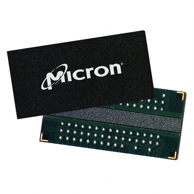
MT47H32M16BT-37E:A TR
| Part Description |
IC DRAM 512MBIT PAR 92FBGA |
|---|---|
| Quantity | 1,477 Available (as of June 15, 2026) |
| Product Category | Memory |
|---|---|
| Manufacturer | Micron Technology Inc. |
| Manufacturing Status | Obsolete |
| Manufacturer Standard Lead Time | Contact Us |
| Datasheet |
Specifications & Environmental
| Device Package | 92-FBGA (11x19) | Memory Format | DRAM | Technology | SDRAM - DDR2 | ||
|---|---|---|---|---|---|---|---|
| Memory Size | 512 Mbit | Access Time | 500 ps | Grade | Commercial (Extended) | ||
| Clock Frequency | 267 MHz | Voltage | 1.7V ~ 1.9V | Memory Type | Volatile | ||
| Operating Temperature | 0°C ~ 85°C (TC) | Write Cycle Time Word Page | 15 ns | Packaging | 92-TFBGA | ||
| Mounting Method | Volatile | Memory Interface | Parallel | Memory Organization | 32M x 16 | ||
| Moisture Sensitivity Level | 5 (48 Hours) | RoHS Compliance | ROHS3 Compliant | REACH Compliance | REACH Unaffected | ||
| Qualification | N/A | ECCN | EAR99 | HTS Code | 8542.32.0024 |
Overview of MT47H32M16BT-37E:A TR – IC DRAM 512MBIT PAR 92FBGA
The MT47H32M16BT-37E:A TR is a 512 Mbit DDR2 SDRAM organized as 32M × 16 with a parallel memory interface in a 92-ball TFBGA package. It implements DDR2 architecture and on-die features described in the Micron datasheet to provide synchronous, high-throughput volatile memory.
Designed for board-level memory integration, the device targets systems that require a compact FBGA footprint, programmable timing options, and operation within a 1.7 V–1.9 V supply window and 0 °C–85 °C temperature range.
Key Features
- Core / Memory Architecture — DDR2 SDRAM organized as 32M × 16 (512 Mbit) with four internal banks for concurrent operation.
- Performance & Timing — Supports programmable CAS latency (CL = 3 and 4) and posted CAS additive latency (AL = 0–4). Speed-grade -37E timing is documented in the datasheet (cycle time 3.75 ns @ CL = 4 for the -37E grade).
- Data Path / Interface — Parallel memory interface with DDR2 differential data strobe options (DQS/DQS#) and optional duplicate output strobe (RDQS) for x8 configurations.
- Signal Integrity & Control — On-die termination (ODT) and an internal DLL to align DQ and DQS transitions with CK; adjustable data-output drive strength.
- Power — Low-voltage operation with supply range of 1.7 V to 1.9 V; VDD/VDDQ referenced to 1.8 V ±0.1 V in the datasheet.
- Refresh & Reliability — JEDEC-defined refresh behavior including 8,192-cycle refresh and 64 ms refresh periods as documented in the datasheet.
- Package & Temperature — 92-ball TFBGA package (92-FBGA, 11 mm × 19 mm footprint) and an operating temperature range of 0 °C to 85 °C (TC).
- Additional DDR2 Features — Four-bit prefetch architecture, programmable burst lengths (4 or 8), and write timing relationships documented by Micron.
Typical Applications
- Embedded memory subsystems — Provides board-level DDR2 memory capacity (512 Mbit) in a compact 92-ball FBGA package for space-constrained designs.
- Interface and buffering — Parallel DDR2 interface and on-die termination support use as buffer memory where programmable timing and drive strength are required.
- Consumer and industrial electronics — Suitable for systems operating within 0 °C to 85 °C that require a 1.7 V–1.9 V low-voltage DDR2 memory solution.
Unique Advantages
- Compact FBGA footprint: 92-ball TFBGA (11 mm × 19 mm) minimizes board area while providing a 32M × 16 memory organization.
- Flexible timing configuration: Programmable CAS latency (CL) and additive latency (AL) options let designers tune read/write timing to match system requirements.
- Signal integrity features: On-die termination, DLL alignment of DQ/DQS, and adjustable output drive strength simplify high-speed interface design.
- Low-voltage operation: 1.7 V–1.9 V supply range (VDD/VDDQ ~1.8 V) supports lower-power system designs using DDR2 signaling levels.
- Documented DDR2 options: Datasheet specifies speed-grade timing and DDR2 features (burst lengths, prefetch, refresh) for predictable system integration.
Why Choose IC DRAM 512MBIT PAR 92FBGA?
This MT47H32M16BT-37E:A TR DDR2 SDRAM balances compact packaging, documented DDR2 timing options, and on-die signal features for board-level memory integration. Its 512 Mbit density in a 32M × 16 organization, combined with programmable latency and ODT, makes it suitable for designs that require a low-voltage parallel DDR2 memory device within the specified temperature range.
Engineers specifying this device can leverage the documented speed-grade and timing options, package dimensions, and supply/temperature limits to assess fit for their system memory requirements and to plan PCB integration accordingly.
Request a quote or submit a pricing inquiry to evaluate the MT47H32M16BT-37E:A TR for your next design.