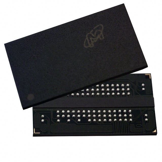
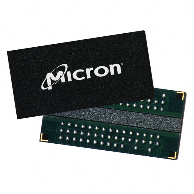
MT47H32M16CC-3:B TR
| Part Description |
IC DRAM 512MBIT PARALLEL 84FBGA |
|---|---|
| Quantity | 15 Available (as of June 15, 2026) |

| Product Category | Memory |
|---|---|
| Manufacturer | Micron Technology Inc. |
| Manufacturing Status | Obsolete |
| Manufacturer Standard Lead Time | Contact Us |
| Datasheet |
Specifications & Environmental
| Device Package | 84-FBGA (12x12.5) | Memory Format | DRAM | Technology | SDRAM - DDR2 | ||
|---|---|---|---|---|---|---|---|
| Memory Size | 512 Mbit | Access Time | 450 ps | Grade | Commercial (Extended) | ||
| Clock Frequency | 333 MHz | Voltage | 1.7V ~ 1.9V | Memory Type | Volatile | ||
| Operating Temperature | 0°C ~ 85°C (TC) | Write Cycle Time Word Page | 15 ns | Packaging | 84-TFBGA | ||
| Mounting Method | Volatile | Memory Interface | Parallel | Memory Organization | 32M x 16 | ||
| Moisture Sensitivity Level | 5 (48 Hours) | RoHS Compliance | ROHS Compliant | REACH Compliance | REACH Unaffected | ||
| Qualification | N/A | ECCN | EAR99 | HTS Code | 8542.32.0024 |
Overview of MT47H32M16CC-3:B TR – IC DRAM 512MBIT PARALLEL 84FBGA
The MT47H32M16CC-3:B TR is a 512 Mbit DDR2 SDRAM organized as 32M × 16 in an 84-ball FBGA package. It implements DDR2 SDRAM architecture with a parallel memory interface and is designed for commercial-temperature systems (0°C to 85°C).
Key capabilities include a 1.8 V nominal supply range, DDR2 timing features such as programmable CAS latency and DLL alignment, and support for selectable burst lengths and on-die termination for synchronous high-speed operation.
Key Features
- Memory Type & Architecture DDR2 SDRAM, 512 Mbit organized as 32M × 16 with 4 internal banks and a 4n-bit prefetch architecture.
- Performance & Timing Clock frequency specified at 333 MHz with an access time of 450 ps and a write cycle time (word page) of 15 ns; programmable CAS latency and posted CAS additive latency are supported.
- Data Integrity & Interface Parallel memory interface with differential data strobe (DQS/DQS#) option and DLL to align DQ and DQS transitions with CK.
- Power & Voltage VDD = +1.8 V ±0.1 V (specified supply range 1.7 V to 1.9 V) with JEDEC-standard 1.8 V I/O (SSTL_18-compatible).
- Burst & Refresh Selectable burst lengths of 4 or 8 and a 64 ms, 8,192-cycle refresh for retained data integrity.
- On-Die Features On-die termination (ODT) and adjustable data-output drive strength to optimize signal integrity.
- Package & Mounting 84-ball TFBGA (84-FBGA) package; supplier package dimensions listed as 84-FBGA (12 mm × 12.5 mm).
- Operating Temperature Commercial temperature range: 0°C to 85°C (T_C).
Typical Applications
- Commercial embedded systems — Provides 512 Mbit of parallel DDR2 memory in a compact 84-FBGA package for space-constrained commercial designs operating from 0°C to 85°C.
- Synchronous memory subsystems — Used where DDR2 timing features such as DLL, programmable CAS latency, and selectable burst lengths are required for aligned high-speed transfers.
- Board-level DRAM solutions — Offers x16 organization and on-die termination for integration into board designs requiring a parallel DDR2 SDRAM device at 1.8 V I/O levels.
Unique Advantages
- Dense x16 organization: 32M × 16 configuration delivers a 512 Mbit footprint suitable for mid-density memory requirements.
- JEDEC-compatible 1.8 V operation: Nominal VDD at +1.8 V ±0.1 V simplifies interface design with SSTL_18-compatible I/O.
- Signal integrity features: On-die termination and adjustable drive strength help optimize board-level signal integrity without external termination networks.
- Flexible timing control: Programmable CAS latency, DLL alignment, and selectable burst lengths (4 or 8) enable timing optimization for different system throughput needs.
- Compact FBGA package: 84-ball FBGA (12 mm × 12.5 mm) provides a small footprint for high-density board layouts.
- Robust refresh management: 64 ms, 8,192-cycle refresh supports standard DDR2 refresh requirements for reliable data retention.
Why Choose IC DRAM 512MBIT PARALLEL 84FBGA?
The MT47H32M16CC-3:B TR delivers a commercially rated DDR2 SDRAM solution with 512 Mbit density, programmable timing features, and signal-integrity options such as on-die termination and DLL alignment. Its 1.8 V supply and 84-FBGA package make it suitable for compact, board-level memory applications that require parallel DDR2 performance within a 0°C to 85°C operating range.
This device is appropriate for designers needing a mid-density DDR2 memory component with flexible timing control and integration-friendly package characteristics, offering predictable electrical and timing behavior tied directly to the provided specifications.
Request a quote or contact sales to inquire about availability, lead times, and pricing for the MT47H32M16CC-3:B TR.