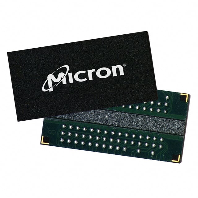
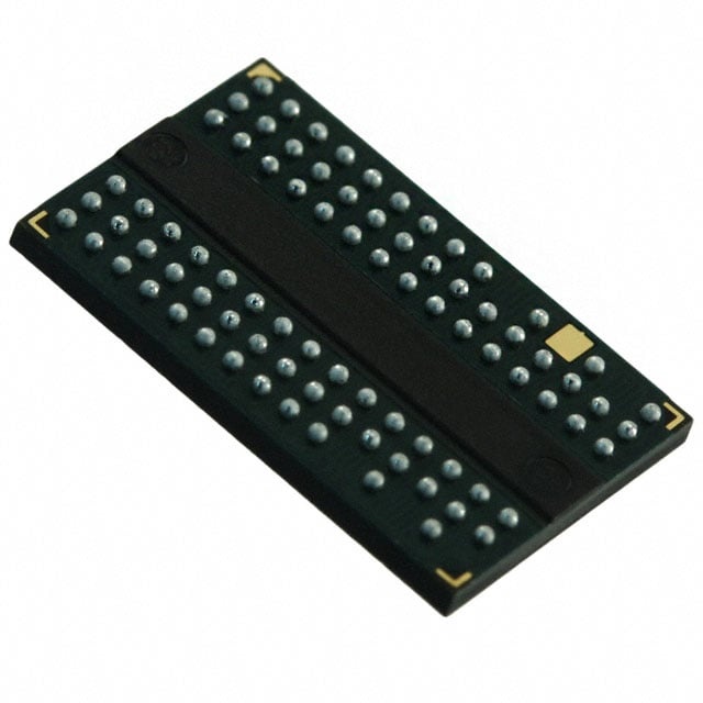
MT47H32M16CC-5E L:B
| Part Description |
IC DRAM 512MBIT PARALLEL 84FBGA |
|---|---|
| Quantity | 700 Available (as of June 18, 2026) |

| Product Category | DRAM Memory |
|---|---|
| Manufacturer | Micron Technology Inc. |
| Manufacturing Status | Obsolete |
| Manufacturer Standard Lead Time | Contact Us |
| Datasheet |
Specifications & Environmental
| Device Package | 84-FBGA (12x12.5) | Memory Format | DRAM | Technology | SDRAM - DDR2 | ||
|---|---|---|---|---|---|---|---|
| Memory Size | 512 Mbit | Access Time | 600 ps | Grade | Commercial (Extended) | ||
| Clock Frequency | 200 MHz | Voltage | 1.7V ~ 1.9V | Memory Type | Volatile | ||
| Operating Temperature | 0°C ~ 85°C (TC) | Write Cycle Time Word Page | 15 ns | Packaging | 84-TFBGA | ||
| Mounting Method | Volatile | Memory Interface | Parallel | Memory Organization | 32M x 16 | ||
| Moisture Sensitivity Level | 3 (168 Hours) | RoHS Compliance | ROHS3 Compliant | REACH Compliance | REACH Unaffected | ||
| Qualification | N/A | ECCN | EAR99 | HTS Code | 8542.32.0024 |
Overview of MT47H32M16CC-5E L:B – IC DRAM 512MBIT PARALLEL 84FBGA
The MT47H32M16CC-5E L:B is a 512 Mbit DDR2 SDRAM organized as 32M × 16 with a parallel memory interface in an 84-ball FBGA package. It implements DDR2 architecture with features such as internal banks, DLL alignment, selectable burst lengths and JEDEC‑standard 1.8V I/O to serve high-throughput buffering and working-memory requirements in commercial-temperature designs.
Key Features
- Core / Memory Architecture DDR2 SDRAM organized as 32M × 16 (512 Mbit) with 4 internal banks for concurrent operation.
- Performance 200 MHz clock frequency (DDR2), 600 ps access time and 15 ns write cycle time (word page) for predictable data timing.
- Timing and Transfer Programmable CAS latency and selectable burst lengths (4 or 8) with DLL to align DQ and DQS transitions for controlled timing behavior.
- Interface and Signal Integrity JEDEC‑standard 1.8V I/O (SSTL_18‑compatible), differential data strobe (DQS/DQS#) option, on‑die termination (ODT) and adjustable data‑output drive strength.
- Power Operating VDD/VDDQ range of 1.7 V to 1.9 V (nominal +1.8 V ±0.1 V) for low-voltage DDR2 operation.
- Refresh and Reliability Standard 64 ms / 8,192‑cycle refresh and internal bank architecture to support sustained operation and data integrity.
- Package and Temperature 84‑TFBGA (84‑ball FBGA, 12 mm × 12.5 mm) package; commercial operating temperature 0°C to 85°C (T_C).
- Options and Compliance Datasheet lists available options including industrial and automotive temperature variants and RoHS compliance as device options.
Typical Applications
- Commercial embedded systems — Provides 512 Mbit parallel DDR2 memory for system working memory and buffering in commercial‑temperature designs.
- Board‑level memory expansion — Compact 84‑ball FBGA package and 1.8 V I/O make the device suitable for mid‑density memory implementations on PCB assemblies.
- High‑throughput buffering — DDR2 architecture with selectable burst lengths and internal banks supports high‑rate data buffering and short latency transfers.
Unique Advantages
- Low‑voltage DDR2 operation: 1.7 V–1.9 V VDD/VDDQ range (nominal 1.8 V) reduces power envelope compared with higher‑voltage memories.
- Deterministic timing options: Programmable CAS latency, DLL alignment and selectable burst lengths enable designers to match timing to system requirements.
- Signal integrity features: On‑die termination, differential DQS option and adjustable output drive strength help optimize signal performance on parallel memory buses.
- Compact FBGA package: 84‑ball FBGA (12 mm × 12.5 mm) enables board‑level density while maintaining ball grid interconnect for reliable mounting.
- Standard refresh scheme: 64 ms / 8,192‑cycle refresh supports standard DRAM refresh management for sustained data retention.
Why Choose MT47H32M16CC-5E L:B?
The MT47H32M16CC-5E L:B delivers a mid‑density (512 Mbit) DDR2 SDRAM solution with a combination of low‑voltage operation, programmable timing and signal‑integrity features tailored for commercial‑temperature system designs. Its 32M × 16 organization, DLL alignment and selectable burst lengths provide designers predictable timing control for buffering and working‑memory roles.
This device is appropriate for designs that require a compact FBGA package, JEDEC‑standard 1.8 V I/O and the standard DDR2 feature set. Options documented in the device datasheet (including industrial and automotive temperature variants and RoHS compliance) support broader supply and deployment choices where specified.
Request a quote or submit an inquiry for pricing and availability of MT47H32M16CC-5E L:B to evaluate integration into your design.