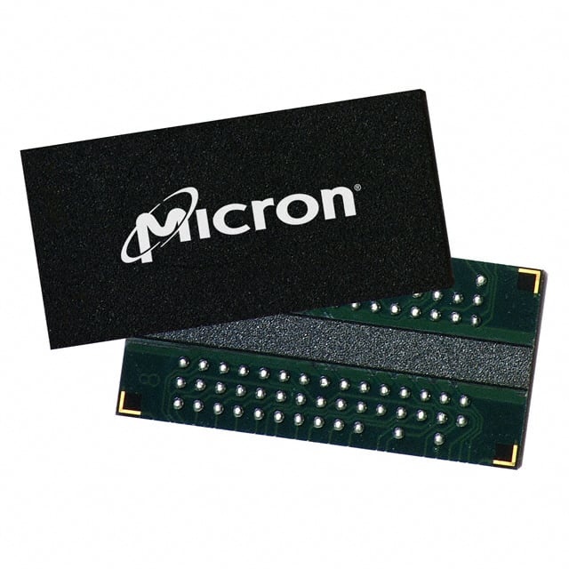
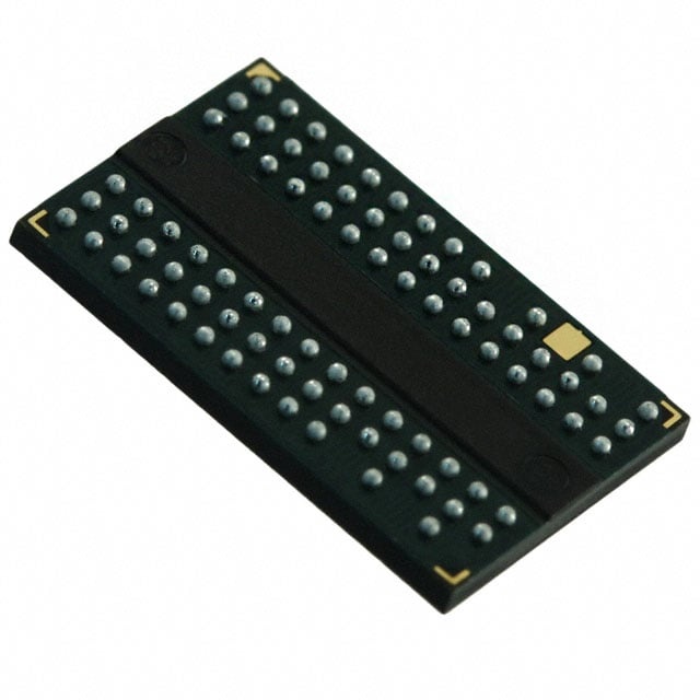
MT47H32M16HR-187E:G
| Part Description |
IC DRAM 512MBIT PAR 84FBGA |
|---|---|
| Quantity | 1,012 Available (as of June 9, 2026) |
| Product Category | Memory |
|---|---|
| Manufacturer | Micron Technology Inc. |
| Manufacturing Status | Obsolete |
| Manufacturer Standard Lead Time | Contact Us |
| Datasheet |
Specifications & Environmental
| Device Package | 84-FBGA (8x12.5) | Memory Format | DRAM | Technology | SDRAM - DDR2 | ||
|---|---|---|---|---|---|---|---|
| Memory Size | 512 Mbit | Access Time | 350 ps | Grade | Commercial (Extended) | ||
| Clock Frequency | 533 MHz | Voltage | 1.7V ~ 1.9V | Memory Type | Volatile | ||
| Operating Temperature | 0°C ~ 85°C (TC) | Write Cycle Time Word Page | 15 ns | Packaging | 84-TFBGA | ||
| Mounting Method | Volatile | Memory Interface | Parallel | Memory Organization | 32M x 16 | ||
| Moisture Sensitivity Level | 3 (168 Hours) | RoHS Compliance | ROHS3 Compliant | REACH Compliance | REACH Unaffected | ||
| Qualification | N/A | ECCN | EAR99 | HTS Code | 8542.32.0028 |
Overview of MT47H32M16HR-187E:G – IC DRAM 512MBIT PAR 84FBGA
The MT47H32M16HR-187E:G is a 512 Mbit DDR2 SDRAM organized as 32M × 16 with a parallel memory interface in an 84-ball FBGA package. It implements DDR2 SDRAM core architecture with a 4n-bit prefetch and 4 internal banks for concurrent operation.
Designed for commercial-temperature systems, the device operates from 1.7 V to 1.9 V (typical 1.8 V I/O) and targets applications that require JEDEC-standard 1.8 V I/O, selectable burst lengths, and on-die termination for signal integrity.
Key Features
- Memory Type & Organization 512 Mbit DDR2 SDRAM organized as 32M × 16 with 4 internal banks and a parallel memory interface.
- Performance Clock frequency specification at 533 MHz and an access time of 350 ps; write cycle time (word page) of 15 ns for predictable timing.
- Voltage & I/O 1.7 V to 1.9 V supply range (VDD = 1.8 V ±0.1 V) with JEDEC‑standard 1.8 V I/O signaling.
- DDR2 Architectural Features 4n-bit prefetch architecture, programmable CAS latency and posted CAS additive latency, selectable burst lengths of 4 or 8, and DLL alignment of DQ/DQS transitions with CK.
- Signal Integrity & Drive On-die termination (ODT) and adjustable data-output drive strength to aid high-speed board implementations; differential data strobe (DQS/DQS#) option available.
- Reliability & Refresh 64 ms, 8192-cycle refresh and support for JEDEC clock jitter specifications to maintain data integrity over standard refresh intervals.
- Package & Temperature 84-ball TFBGA package (8.0 mm × 12.5 mm) specified for commercial temperature operation (0°C to 85°C TC).
Typical Applications
- System Memory for Embedded Platforms Use as parallel DDR2 system memory where a 512 Mbit, 32M × 16 organization and JEDEC 1.8 V I/O are required.
- High‑Speed Buffering Suitable for designs needing selectable burst lengths and on-die termination to support controlled high-speed data transfers.
- Compact PCB Implementations The 84‑ball FBGA (8 × 12.5 mm) package supports dense board layouts requiring surface-mount DRAM components.
Unique Advantages
- JEDEC‑Standard 1.8 V I/O: Ensures compatibility with systems designed for SSTL_18-compatible signaling and a 1.8 V power domain.
- Flexible Timing Options: Programmable CAS latency and selectable burst lengths (4 or 8) allow tailoring latency and burst behavior to system needs.
- Signal Integrity Features: On-die termination, differential DQS options and adjustable drive strength help maintain reliable high-speed interfaces.
- Compact FBGA Package: 84-ball FBGA (8 × 12.5 mm) enables compact board integration while providing the necessary ballout for parallel DDR2 connections.
- Commercial Temperature Rating: Specified operation from 0°C to 85°C (TC) for use in standard commercial applications.
- Controlled Power Envelope: Narrow supply range (1.7 V–1.9 V) simplifies power rail design for 1.8 V systems.
Why Choose IC DRAM 512MBIT PAR 84FBGA?
The MT47H32M16HR-187E:G brings DDR2 SDRAM architecture in a 512 Mbit x16 configuration suitable for commercial-temperature systems that require JEDEC 1.8 V I/O, selectable burst operation, and on-die termination. Its combination of programmable latency, DDR2 prefetch architecture and FBGA packaging facilitates compact, high-speed parallel memory designs.
This device is appropriate for designs that need predictable DDR2 timing (533 MHz specification and 350 ps access time), tight power domain control (1.7 V–1.9 V), and board-density advantages provided by an 84-ball FBGA package.
Request a quote or submit an inquiry to obtain pricing, availability, and integration support for the MT47H32M16HR-187E:G.