MT47H32M16HR-25E IT:G
| Part Description |
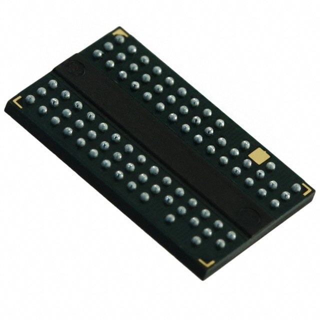
IC DRAM 512MBIT PARALLEL 84FBGA |
|---|---|
| Quantity | 1,736 Available (as of June 15, 2026) |

| Product Category | Memory |
|---|---|
| Manufacturer | Micron Technology Inc. |
| Manufacturing Status | Obsolete |
| Manufacturer Standard Lead Time | Contact Us |
| Datasheet |
Specifications & Environmental
| Device Package | 84-FBGA (8x12.5) | Memory Format | DRAM | Technology | SDRAM - DDR2 | ||
|---|---|---|---|---|---|---|---|
| Memory Size | 512 Mbit | Access Time | 400 ps | Grade | Automotive | ||
| Clock Frequency | 400 MHz | Voltage | 1.7V ~ 1.9V | Memory Type | Volatile | ||
| Operating Temperature | -40°C ~ 95°C (TC) | Write Cycle Time Word Page | 15 ns | Packaging | 84-TFBGA | ||
| Mounting Method | Volatile | Memory Interface | Parallel | Memory Organization | 32M x 16 | ||
| Moisture Sensitivity Level | 3 (168 Hours) | RoHS Compliance | ROHS Compliant | REACH Compliance | REACH Unaffected | ||
| Qualification | N/A | ECCN | EAR99 | HTS Code | 8542.32.0028 |
Overview of MT47H32M16HR-25E IT:G – IC DRAM 512MBIT PARALLEL 84FBGA
The MT47H32M16HR-25E IT:G is a 512 Mbit DDR2 SDRAM device in a 84-ball FBGA package offering a parallel x16 interface. It implements a 32M × 16 organization with DDR2 architecture and JEDEC-standard 1.8 V I/O.
Designed for systems that require compact, low-voltage, industrial-temperature memory, this device delivers DDR2 performance up to the -25E timing grade while providing features that support signal integrity and flexible memory timing.
Key Features
- Memory Core 512 Mbit DDR2 SDRAM organized as 32M × 16 with 4 internal banks for concurrent operation.
- Performance DDR2 SDRAM technology with a specified clock frequency of 400 MHz and part timing corresponding to the -25E timing grade (2.5 ns @ CL = 5 / DDR2-800 option listed in the product datasheet).
- Voltage and I/O VDD = 1.8 V ± 0.1 V, VDDQ = 1.8 V ± 0.1 V with JEDEC‑standard 1.8 V I/O (SSTL_18‑compatible).
- Timing and Latency Programmable CAS latency and posted CAS additive latency; selectable burst lengths of 4 or 8; WRITE latency = READ latency − 1 CK.
- Signal Integrity DLL to align DQ and DQS with CK, on‑die termination (ODT), differential data strobe (DQS/DQS#) option and adjustable data‑output drive strength.
- Refresh and Reliability 64 ms, 8192‑cycle refresh and support for JEDEC clock jitter specification as documented in the datasheet.
- Package & Mounting 84‑ball FBGA (8 mm × 12.5 mm) package (84‑TFBGA / 84‑FBGA) intended for surface mount PCB integration.
- Operating Range Industrial temperature option with device temperature range listed as −40 °C to 95 °C (TC) for qualified industrial use.
- Standards & Compliance Device datasheet lists RoHS‑compliant construction and JEDEC‑compatible interfaces and timing options.
- Other Electricals Parallel memory interface, access timing examples include 400 ps access time and write cycle time (word page) of 15 ns as specified in the product data.
Typical Applications
- Embedded systems Local DRAM for embedded boards and modules that require a parallel DDR2 x16 memory with industrial temperature capability.
- Industrial control Memory for automation and control equipment operating across a wide temperature range where a compact FBGA package is required.
- System buffers and data storage Frame buffers, data buffers and temporary storage in designs using DDR2 parallel memory architectures.
Unique Advantages
- Compact FBGA footprint: 84‑ball FBGA (8 × 12.5 mm) minimizes PCB area for space‑constrained designs.
- Low‑voltage operation: 1.8 V nominal VDD/VDDQ reduces power supply complexity for DDR2 systems.
- Industrial temperature support: −40 °C to 95 °C (TC) rating supports deployments in harsher ambient environments.
- Flexible performance tuning: Programmable CAS latency, selectable burst length and adjustable drive strength allow tuning to system timing and signal integrity needs.
- Signal integrity features: DLL, on‑die termination and differential DQS options help maintain data timing and reliability at DDR2 speeds.
- Clear timing definition: Part includes -25E timing grade information (2.5 ns @ CL = 5) and documented access/write cycle timings for predictable system integration.
Why Choose MT47H32M16HR-25E IT:G?
The MT47H32M16HR-25E IT:G positions itself as a straightforward 512 Mbit DDR2 SDRAM solution for designers needing a parallel x16 memory in a compact 84‑ball FBGA package with industrial temperature support. Its JEDEC‑compatible I/O, programmable timing and on‑die signal integrity features make it suitable for embedded and industrial applications where controlled DDR2 performance and board footprint are priorities.
This device is appropriate for design teams specifying low‑voltage DDR2 memory (1.8 V) with documented timing grades and refresh behavior, and for projects that benefit from selectable latency and burst options to match system timing requirements.
Request a quote or submit an inquiry to receive pricing, availability and technical support information for the MT47H32M16HR-25E IT:G.