
MT47H32M16HR-25E L:G
| Part Description |
IC DRAM 512MBIT PARALLEL 84FBGA |
|---|---|
| Quantity | 1,202 Available (as of June 14, 2026) |
| Product Category | Memory |
|---|---|
| Manufacturer | Micron Technology Inc. |
| Manufacturing Status | Obsolete |
| Manufacturer Standard Lead Time | Contact Us |
| Datasheet |
Specifications & Environmental
| Device Package | 84-FBGA (8x12.5) | Memory Format | DRAM | Technology | SDRAM - DDR2 | ||
|---|---|---|---|---|---|---|---|
| Memory Size | 512 Mbit | Access Time | 400 ps | Grade | Commercial (Extended) | ||
| Clock Frequency | 400 MHz | Voltage | 1.7V ~ 1.9V | Memory Type | Volatile | ||
| Operating Temperature | 0°C ~ 85°C (TC) | Write Cycle Time Word Page | 15 ns | Packaging | 84-TFBGA | ||
| Mounting Method | Volatile | Memory Interface | Parallel | Memory Organization | 32M x 16 | ||
| Moisture Sensitivity Level | 3 (168 Hours) | RoHS Compliance | ROHS Compliant | REACH Compliance | REACH Unaffected | ||
| Qualification | N/A | ECCN | EAR99 | HTS Code | 8542.32.0028 |
Overview of MT47H32M16HR-25E L:G – IC DRAM 512MBIT PARALLEL 84FBGA
The MT47H32M16HR-25E L:G is a 512 Mbit DDR2 SDRAM organized as 32M × 16 with a parallel memory interface supplied in an 84-ball FBGA package. It implements DDR2 architecture with a 4n-bit prefetch and four internal banks to support standard DDR2 command/response timing and burst transfers.
This device targets designs that require a compact, parallel DDR2 memory component with 1.8 V class operation, programmable latency and selectable burst lengths for controlled throughput and timing behavior.
Key Features
- Memory Architecture 512 Mbit DDR2 SDRAM organized as 32M × 16 with 4 internal banks and 4n-bit prefetch architecture for standard DDR2 operation.
- Performance / Timing Clock frequency specified at 400 MHz with an access time of 400 ps; programmable CAS latency and selectable burst lengths (4 or 8) to match system timing requirements.
- Power Supply VDD = +1.8 V ±0.1 V (documented as 1.7 V–1.9 V supply range) supporting JEDEC-standard 1.8 V I/O (SSTL_18-compatible).
- Signal Integrity Built-in DLL to align DQ and DQS transitions with CK and on-die termination (ODT) to aid signal integrity on parallel interfaces.
- Data I/O Differential data strobe (DQS/DQS#) option to support DDR2 data capture and timing alignment.
- Refresh and Reliability 64 ms, 8192-cycle refresh scheme as defined for the device family.
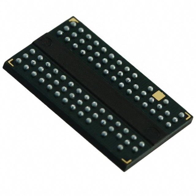
- Package and Mounting 84-ball TFBGA package (8 mm × 12.5 mm) in FBGA format for board-level mounting and compact footprint.
- Operating Temperature Commercial temperature range documented at 0 °C to 85 °C (TC).
- Options and Family Features Family-level options include adjustable data-output drive strength and support for JEDEC clock jitter specifications; industrial and automotive options are noted in the product family documentation.
- Standards Compliance Device family supports JEDEC-standard 1.8 V I/O signaling and is listed as RoHS-compliant in the datasheet material for the DDR2 512Mb family.
Typical Applications
- Parallel DDR2 memory subsystems Used where a 512 Mbit, x16 parallel DDR2 component is required for system memory implementations on PCBs with FBGA footprint constraints.
- Compact board-level integration Suited to designs needing a high-density DRAM device in an 84-ball FBGA (8 mm × 12.5 mm) package.
- Timing-sensitive data buffering Applicable in systems that leverage programmable CAS latency, selectable burst lengths and DLL alignment for controlled read/write timing.
Unique Advantages
- Standard DDR2 interface: Enables direct integration into designs requiring JEDEC 1.8 V DDR2 signaling and differential DQS-based data capture.
- Flexible timing and burst modes: Programmable CAS latency and selectable burst lengths (4 or 8) allow designers to tune latency and transfer granularity for target workloads.
- Signal integrity features: On-die termination (ODT) and an internal DLL help reduce board-level signal tuning and improve timing alignment between DQ/DQS and CK.
- Compact FBGA package: 84-ball FBGA (8 mm × 12.5 mm) reduces PCB area for space-constrained applications while providing the solder-ball connections standard for BGAs.
- 1.8 V low-voltage operation: Narrow supply range (1.7 V–1.9 V) with JEDEC I/O compatibility supports consistent power and I/O behavior across the memory interface.
Why Choose IC DRAM 512MBIT PARALLEL 84FBGA?
The MT47H32M16HR-25E L:G provides a 512 Mbit DDR2 SDRAM solution that combines JEDEC-compatible 1.8 V signaling, programmable timing, on-die termination and an 84-ball FBGA package for compact board integration. Its 32M × 16 organization and four internal banks offer standard DDR2 banking and burst behavior suitable for parallel memory subsystems.
This device is aimed at designs that require a stable, documented DDR2 memory component with configurable timing and signal-integrity features. The product family documentation also outlines options for drive strength, temperature variants and other package revisions for customers needing extended configurations.
Request a quote or contact sales to discuss availability, lead times and pricing for the MT47H32M16HR-25E L:G.


