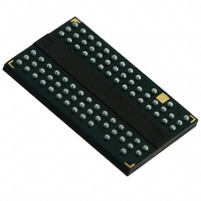
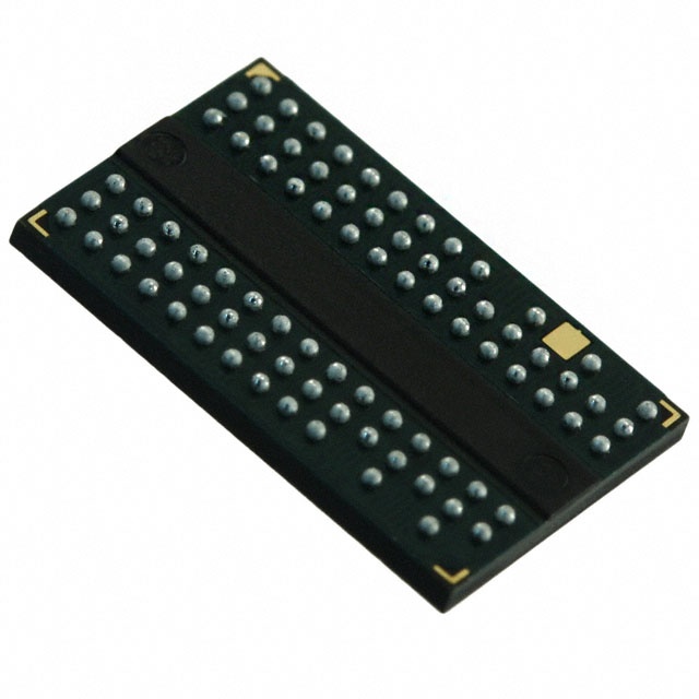
MT47H32M16HR-3:F
| Part Description |
IC DRAM 512MBIT PARALLEL 84FBGA |
|---|---|
| Quantity | 1,176 Available (as of June 15, 2026) |

| Product Category | Memory |
|---|---|
| Manufacturer | Micron Technology Inc. |
| Manufacturing Status | Obsolete |
| Manufacturer Standard Lead Time | Contact Us |
| Datasheet |
Specifications & Environmental
| Device Package | 84-FBGA (8x12.5) | Memory Format | DRAM | Technology | SDRAM - DDR2 | ||
|---|---|---|---|---|---|---|---|
| Memory Size | 512 Mbit | Access Time | 450 ps | Grade | Commercial (Extended) | ||
| Clock Frequency | 333 MHz | Voltage | 1.7V ~ 1.9V | Memory Type | Volatile | ||
| Operating Temperature | 0°C ~ 85°C (TC) | Write Cycle Time Word Page | 15 ns | Packaging | 84-TFBGA | ||
| Mounting Method | Volatile | Memory Interface | Parallel | Memory Organization | 32M x 16 | ||
| Moisture Sensitivity Level | 3 (168 Hours) | RoHS Compliance | ROHS3 Compliant | REACH Compliance | REACH Unaffected | ||
| Qualification | N/A | ECCN | EAR99 | HTS Code | 8542.32.0024 |
Overview of MT47H32M16HR-3:F – IC DRAM 512MBIT PARALLEL 84FBGA
The MT47H32M16HR-3:F is a 512 Mbit DDR2 SDRAM organized as 32M x 16 with a parallel memory interface in an 84-ball FBGA package. It implements DDR2 architecture features such as a DLL, 4 internal banks, selectable burst lengths, and programmable CAS latency.
Designed for systems requiring a 512 Mbit DDR2 x16 device operating from a 1.7 V to 1.9 V supply and a commercial temperature range of 0°C to 85°C, the device targets board-level integration where compact FBGA packaging and JEDEC-standard 1.8 V I/O behavior are required.
Key Features
- Core — DDR2 SDRAM Architecture 4n-bit prefetch architecture with an internal DLL to align DQ and DQS transitions; supports 4 internal banks for concurrent operation and selectable burst lengths of 4 or 8.
- Memory Organization 512 Mbit density arranged as 32M × 16 (8 Meg × 16 × 4 banks); row address A[12:0], column A[9:0] and 8K refresh count as specified for the 32M × 16 configuration.
- Interface & Timing Parallel DDR2 interface with differential data strobe (DQS/DQS#) option and programmable CAS latency; specified clock frequency 333 MHz (DDR2-667 data rate) and an access time of 450 ps.
- Power VDD and VDDQ specifications of +1.8 V ±0.1 V (documented supply range 1.7 V to 1.9 V), with JEDEC-standard 1.8 V I/O (SSTL_18-compatible).
- Signal Integrity & Control On-die termination (ODT), adjustable data-output drive strength, duplicate output strobe (RDQS) option for x8, and support for JEDEC clock jitter specifications.
- Refresh & Reliability 64 ms, 8192-cycle refresh and standard DDR2 reliability features; write latency relationship documented as WRITE latency = READ latency − 1 CK.
- Package & Temperature 84-ball FBGA (8.0 mm × 12.5 mm) package (84-TFBGA / 84-FBGA Rev. F,G HR) with commercial operating temperature range 0°C to 85°C.
Typical Applications
- Systems requiring DDR2 memory — Use as board-level DDR2 SDRAM (512 Mbit, x16) where a parallel DDR2 interface and JEDEC 1.8 V I/O are specified.
- Compact module and board designs — FBGA 84-ball package provides a small footprint option for space-constrained PCBs requiring 512 Mbit DDR2 capacity.
- Designs with 1.8 V power domains — Suited for systems that operate VDD/VDDQ within 1.7 V to 1.9 V and require SSTL_18-compatible signaling.
Unique Advantages
- DDR2 feature set: Built-in DLL, 4n-bit prefetch, selectable burst lengths, and programmable CAS latency provide timing flexibility for system designers.
- JEDEC 1.8 V I/O compatibility: VDD/VDDQ = +1.8 V ±0.1 V supports SSTL_18-compatible signaling for straightforward interface integration.
- On-die termination and drive control: ODT and adjustable data-output drive strength help manage signal integrity on high-speed parallel buses.
- Compact FBGA package: 84-ball FBGA (8.0 mm × 12.5 mm) offers a board-level footprint suited to dense PCB layouts.
- Documented timing options: Specified clock frequency (333 MHz), access time (450 ps), and timing grades in the datasheet enable matched memory subsystem design.
Why Choose MT47H32M16HR-3:F?
The MT47H32M16HR-3:F provides a documented DDR2 SDRAM solution in a 512 Mbit, x16 organization with commercial temperature rating and an 84-ball FBGA package. Its combination of DDR2 architecture features (DLL, ODT, selectable burst lengths, programmable CAS) and 1.8 V I/O compatibility make it suitable for designs that require a standard DDR2 parallel memory device with defined timing and power characteristics.
This device is appropriate for engineers specifying board-level DDR2 memory in systems operating within the documented supply and temperature ranges, offering deterministic refresh behavior and signal-integrity options detailed in the product datasheet.
If you need pricing or availability for MT47H32M16HR-3:F, request a quote or submit an inquiry for a formal price and lead-time response.