MT47H32M16NF-25E:H TR
| Part Description |
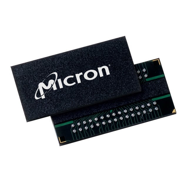
IC DRAM 512MBIT PARALLEL 84FBGA |
|---|---|
| Quantity | 1,720 Available (as of June 15, 2026) |

| Product Category | Memory |
|---|---|
| Manufacturer | Micron Technology Inc. |
| Manufacturing Status | Active |
| Manufacturer Standard Lead Time | 2 Weeks |
| Datasheet |
Specifications & Environmental
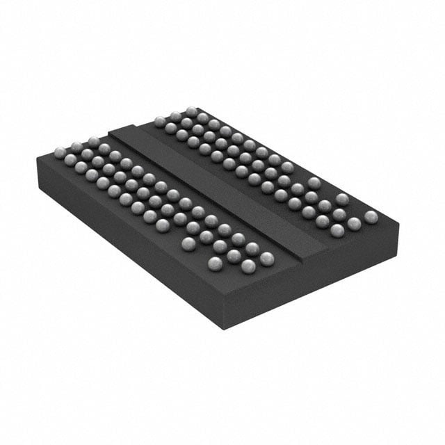
| Device Package | 84-FBGA (8x12.5) | Memory Format | DRAM | Technology | SDRAM - DDR2 | ||
|---|---|---|---|---|---|---|---|
| Memory Size | 512 Mbit | Access Time | 400 ps | Grade | Automotive | ||
| Clock Frequency | 400 MHz | Voltage | 1.7V ~ 1.9V | Memory Type | Volatile | ||
| Operating Temperature | 0°C ~ 85°C (TC) | Write Cycle Time Word Page | 15 ns | Packaging | 84-TFBGA | ||
| Mounting Method | Volatile | Memory Interface | Parallel | Memory Organization | 32M x 16 | ||
| Moisture Sensitivity Level | 3 (168 Hours) | RoHS Compliance | ROHS3 Compliant | REACH Compliance | REACH Unaffected | ||
| Qualification | AEC-Q100 | ECCN | EAR99 | HTS Code | 8542.32.0028 |
Overview of MT47H32M16NF-25E:H TR – IC DRAM 512MBIT PARALLEL 84FBGA
The MT47H32M16NF-25E:H TR is a 512 Mbit DDR2 SDRAM organized as 32M × 16 with a parallel memory interface in an 84-ball FBGA package. It delivers DDR2-class memory architecture with a 4n-bit prefetch design, targeting embedded and automotive electronic modules that require compact, qualified DRAM for system memory and buffering.
With a 1.7 V–1.9 V supply range, 400 MHz clock capability, and AEC‑Q100 qualification, this device is offered for designs requiring automotive-grade qualification and DDR2 performance in a small 8 mm × 12.5 mm FBGA footprint.
Key Features
- Memory Architecture 512 Mbit DDR2 SDRAM organized as 32M × 16 with 4 internal banks and a 4n-bit prefetch architecture for DDR2 operation.
- Performance Supports a 400 MHz clock rate and an access time of 400 ps with selectable burst lengths (4 or 8) and programmable CAS latency.
- Timing Write cycle time (word page) of 15 ns and JEDEC-standard timing options including programmable CAS and additive latency.
- Power Operates from a 1.7 V to 1.9 V supply (VDD and VDDQ), providing standard DDR2 1.8 V I/O compatibility.
- Interface Parallel memory interface with differential data strobe (DQS/DQS#) options and DLL to align DQ/DQS with CK.
- Package 84-ball thin FBGA (8 mm × 12.5 mm) package suitable for compact board designs and high-density routing.
- Operating Range & Qualification Commercial operating temperature range of 0 °C to +85 °C (TC) and AEC‑Q100 qualification for automotive-grade applications.
- System Reliability On-die termination (ODT), selectable data-output drive strength and support for standard refresh cycles (8192-cycle refresh) to maintain signal integrity and data retention.
Typical Applications
- Automotive Electronic Modules Memory and buffering for control units and infotainment subsystems where AEC‑Q100 qualification is required.
- Embedded Systems System memory and high-speed data buffering for compact embedded boards using a parallel DDR2 interface.
- Consumer and Industrial Equipment Low-voltage DDR2 memory for devices needing a small FBGA footprint and standard 1.8 V I/O compatibility.
Unique Advantages
- AEC‑Q100 Qualified: Provides automotive-grade qualification for use in vehicle electronic systems that require recognized component reliability.
- DDR2 Performance at 400 MHz: Enables high-throughput parallel memory operations with programmable latency and selectable burst lengths for flexible memory timing.
- Compact FBGA Package: 84-ball FBGA (8 mm × 12.5 mm) offers a small PCB footprint for space-constrained designs while supporting high-density routing.
- Flexible Voltage Range: 1.7 V–1.9 V supply supports standard DDR2 1.8 V I/O signaling for compatibility with common DDR2 system designs.
- Signal Integrity Features: On-die termination and DLL alignment of DQ/DQS improve timing margins and data eye performance in high-speed designs.
- Industry-Standard DDR2 Options: Programmable CAS, additive latency and selectable burst lengths enable tailoring of memory timing to application requirements.
Why Choose MT47H32M16NF-25E:H TR?
The MT47H32M16NF-25E:H TR combines DDR2 SDRAM architecture, an 84-ball FBGA package, and automotive AEC‑Q100 qualification to provide a compact, qualified memory building block for embedded and vehicle electronics. Its 512 Mbit capacity (32M × 16), 400 MHz clock capability, and configurable timing options make it suitable for designs that require standardized DDR2 performance with automotive-grade reliability.
This device is suited for engineers specifying reliable, low-voltage DDR2 memory in space-constrained PCBs and in applications where component qualification and consistent timing behavior are important for system integration and lifecycle support.
Request a quote or contact sales to discuss availability, pricing, and volume options for the MT47H32M16NF-25E:H TR.