MT47H32M8BP-5E:B
| Part Description |
IC DRAM 256MBIT PARALLEL 60FBGA |
|---|---|
| Quantity | 316 Available (as of June 15, 2026) |
| Product Category | Memory |
|---|---|
| Manufacturer | Micron Technology Inc. |
| Manufacturing Status | Obsolete |
| Manufacturer Standard Lead Time | Contact Us |
| Datasheet |
Specifications & Environmental
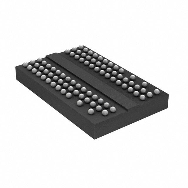
| Device Package | 60-FBGA (8x12) | Memory Format | DRAM | Technology | SDRAM - DDR2 | ||
|---|---|---|---|---|---|---|---|
| Memory Size | 256 Mbit | Access Time | 600 ps | Grade | Commercial (Extended) | ||
| Clock Frequency | 200 MHz | Voltage | 1.7V ~ 1.9V | Memory Type | Volatile | ||
| Operating Temperature | 0°C ~ 85°C (TC) | Write Cycle Time Word Page | 15 ns | Packaging | 60-FBGA | ||
| Mounting Method | Volatile | Memory Interface | Parallel | Memory Organization | 32M x 8 | ||
| Moisture Sensitivity Level | 2 (1 Year) | RoHS Compliance | ROHS3 Compliant | REACH Compliance | REACH Unaffected | ||
| Qualification | N/A | ECCN | EAR99 | HTS Code | 8542.32.0024 |
Overview of MT47H32M8BP-5E:B – IC DRAM 256MBIT PARALLEL 60FBGA
The MT47H32M8BP-5E:B is a 256Mbit DDR2 SDRAM organized as 32M × 8 with a parallel memory interface in a 60-ball FBGA (8×12) package. It implements a DDR2 SDRAM architecture with 4 internal banks and a 4n-bit prefetch, delivering DDR2-400 performance with a 200 MHz clock (400 MT/s data rate).
This device targets designs that require compact, low-voltage DDR2 DRAM for embedded memory subsystems operating in commercial temperature ranges (0°C to 85°C), offering programmable latency, selectable burst lengths and on-die termination for system-level timing and signal integrity control.
Key Features
- DDR2 SDRAM Core 4n-bit prefetch architecture with 4 internal banks for concurrent operation and programmable CAS latency (CL) and additive latency (AL).
- Memory Organization & Capacity 32M × 8 organization providing 256 Mbit total capacity in a parallel DRAM format.
- Performance & Timing Rated for DDR2-400 operation (200 MHz clock, 400 MT/s), example timing for the -5E grade includes a 5.0 ns cycle time; write cycle time (word page) specified at 15 ns and access time at 600 ps.
- Power VDD and VDDQ operate at +1.8 V ±0.1 V (specified supply range 1.7 V to 1.9 V) with JEDEC-standard 1.8 V I/O (SSTL_18-compatible).
- Signal & I/O Options Differential data strobe (DQS/DQS#) option and duplicate output strobe (RDQS) option for x8 devices to aid data capture and timing alignment; DLL aligns DQ and DQS transitions with CK.
- System Reliability & Signal Integrity On-die termination (ODT) and support for JEDEC clock jitter specifications to assist system-level signal integrity and timing margins.
- Burst & Refresh Selectable burst lengths of 4 or 8 and standard 64 ms, 8,192-cycle refresh for data retention management.
- Package & Mechanical 60-ball FBGA (8 mm × 12 mm) package (60-FBGA (8×12)) for compact board real estate and surface-mount assembly.
- Temperature Range Commercial operating temperature range of 0°C to 85°C (TC).
- Compliance Datasheet indicates RoHS compliance and JEDEC-standard I/O compatibility.
Typical Applications
- Embedded Memory Subsystems Use as onboard DDR2 storage in embedded platforms that require a compact 256 Mbit memory element in a 60-FBGA footprint.
- Consumer and Industrial Electronics Integration where commercial temperature operation (0°C to 85°C) and DDR2-400 performance are required for system buffering and working memory.
- Timing-Critical Data Buffers Applications that benefit from programmable CAS latency, selectable burst lengths, and on-die termination to manage read/write timing and signal integrity.
Unique Advantages
- Standard DDR2 Interface: JEDEC-standard 1.8 V I/O and DDR2 signaling simplify integration with existing DDR2 memory controllers.
- Compact FBGA Package: 60-ball FBGA (8×12) enables high-density board designs while maintaining a surface-mount form factor.
- Flexible Timing Control: Programmable CAS and additive latency plus selectable burst lengths allow designers to tune performance for specific system requirements.
- Signal Integrity Features: On-die termination, differential DQS options and DLL alignment reduce external termination needs and assist high-speed timing alignment.
- Low-Voltage Operation: 1.8 V VDD/VDDQ operation (1.7 V–1.9 V specified) supports lower-power system designs compared to legacy higher-voltage memories.
- Documented Speed Grades: Available timing grade (-5E) corresponds to DDR2-400 cycle timing, enabling predictable timing integration in system design.
Why Choose MT47H32M8BP-5E:B?
The MT47H32M8BP-5E:B delivers a compact, standards-based DDR2 SDRAM option with clearly defined timing grades, on-die signal integrity features and low-voltage operation suitable for commercial-temperature embedded designs. Its 32M × 8 organization and 60-FBGA packaging make it straightforward to integrate into space-constrained memory subsystems.
This device is appropriate for designers seeking a documented DDR2-400 memory component with programmable latency, selectable burst modes and ODT for improved timing and signal integrity control. The combination of package size, supply voltage range and JEDEC I/O compatibility supports scalable integration into existing DDR2-capable platforms.
Request a quote or contact sales to discuss availability, lead times and to obtain ordering information for the MT47H32M8BP-5E:B. Reference the full product datasheet for detailed timing, electrical and mechanical specifications.