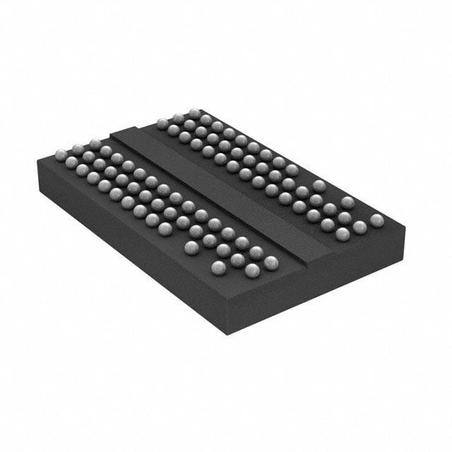
MT47H64M8B6-25:D TR
| Part Description |
IC DRAM 512MBIT PARALLEL 60FBGA |
|---|---|
| Quantity | 224 Available (as of June 8, 2026) |

| Product Category | Memory |
|---|---|
| Manufacturer | Micron Technology Inc. |
| Manufacturing Status | Obsolete |
| Manufacturer Standard Lead Time | Contact Us |
| Datasheet |
Specifications & Environmental
| Device Package | 60-FBGA | Memory Format | DRAM | Technology | SDRAM - DDR2 | ||
|---|---|---|---|---|---|---|---|
| Memory Size | 512 Mbit | Access Time | 400 ps | Grade | Commercial (Extended) | ||
| Clock Frequency | 400 MHz | Voltage | 1.7V ~ 1.9V | Memory Type | Volatile | ||
| Operating Temperature | 0°C ~ 85°C (TC) | Write Cycle Time Word Page | 15 ns | Packaging | 60-FBGA | ||
| Mounting Method | Volatile | Memory Interface | Parallel | Memory Organization | 64M x 8 | ||
| Moisture Sensitivity Level | 3 (168 Hours) | RoHS Compliance | ROHS3 Compliant | REACH Compliance | REACH Unaffected | ||
| Qualification | N/A | ECCN | 3A991B2A | HTS Code | 8542.32.0024 |
Overview of MT47H64M8B6-25:D TR – IC DRAM 512MBIT PARALLEL 60FBGA
The MT47H64M8B6-25:D TR is a 512 Mbit DDR2 SDRAM device manufactured by Micron Technology Inc., organized as 64M x 8 with a parallel memory interface. It implements DDR2 architecture and is offered in a 60‑ball FBGA package for compact board-level integration.
This device targets designs that require low-voltage (+1.8V ±0.1V) DDR2 memory at a 400 MHz clock frequency, providing programmable timing options and selectable burst lengths to match system timing and throughput requirements.
Key Features
- Core / Architecture DDR2 SDRAM architecture with 4‑bit prefetch and an internal DLL to align DQ and DQS transitions with CK.
- Memory Organization 512 Mbit capacity organized as 64M × 8 with 4 internal banks (16 Meg × 8 × 4 banks as listed in datasheet).
- Performance & Timing Rated for a 400 MHz clock frequency and 400 ps access time; programmable CAS latency and selectable burst lengths (4 or 8). Write cycle time (word page) is specified at 15 ns.
- Power & I/O VDD / VDDQ operating range +1.7 V to +1.9 V (JEDEC-standard 1.8 V I/O, SSTL_18-compatible as documented in the datasheet).
- Signal & Drive Options Differential data strobe (DQS/DQS#) option, duplicate output strobe (RDQS) option for x8 configuration, and adjustable data-output drive strength.
- System Reliability On‑die termination (ODT) and standard 8,192‑cycle (8K) refresh support with a 64 ms refresh interval.
- Package & Temperature Supplied in a 60‑ball FBGA package; the supplied commercial operating temperature range is 0°C to 85°C (T_C).
- Compliance RoHS compliant as stated in the datasheet.
Typical Applications
- Embedded memory expansion — Provides a 512 Mbit DDR2 parallel memory option for designs that require on‑board SDRAM in a 60‑ball FBGA footprint.
- Compact system modules — Small FBGA package supports space‑constrained board designs that need low‑voltage DDR2 memory at 400 MHz clocking.
- Legacy DDR2 parallel designs — Suitable for systems that implement DDR2 SDRAM parallel interfaces with programmable CAS and selectable burst length requirements.
Unique Advantages
- Standard DDR2 interface at 1.8 V — Operates within a +1.7 V to +1.9 V supply window, matching JEDEC 1.8 V I/O expectations.
- Programmable timing flexibility — Programmable CAS latency and selectable burst lengths allow tuning for different system timing and throughput needs.
- Compact FBGA packaging — 60‑ball FBGA package enables dense board placement while providing the full 512 Mbit DDR2 function.
- On‑die termination and drive options — ODT plus adjustable drive strength and strobe options reduce external termination complexity and support signal integrity tuning.
- Micron product backing — Part of Micron’s 512 Mb DDR2 device family with documented speed grades and package options in the datasheet.
Why Choose IC DRAM 512MBIT PARALLEL 60FBGA?
The MT47H64M8B6-25:D TR delivers a 512 Mbit DDR2 SDRAM option with programmable timing, 4‑bank architecture, and a 60‑ball FBGA package suitable for compact, low‑voltage designs. Its 400 MHz clock rating, on‑die termination, and drive/strobe options offer the configuration flexibility needed to match system timing and signal integrity requirements.
This device is appropriate for engineers specifying parallel DDR2 memory where a 64M × 8 organization, commercial temperature operation (0°C–85°C), and +1.8 V operation are required. It provides a verifiable set of features and timing options documented by the manufacturer for integration into existing DDR2 system architectures.
Request a quote or submit an inquiry to obtain pricing and availability for the MT47H64M8B6-25:D TR.