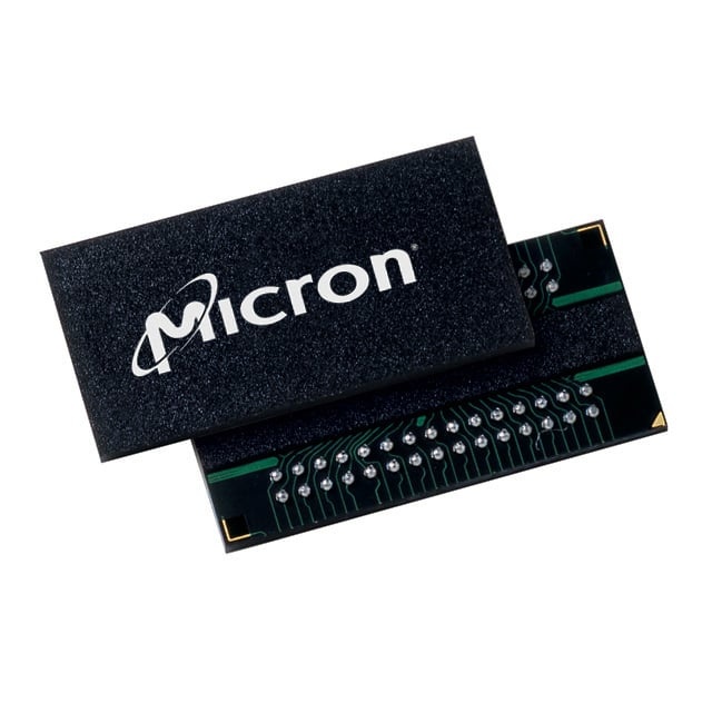
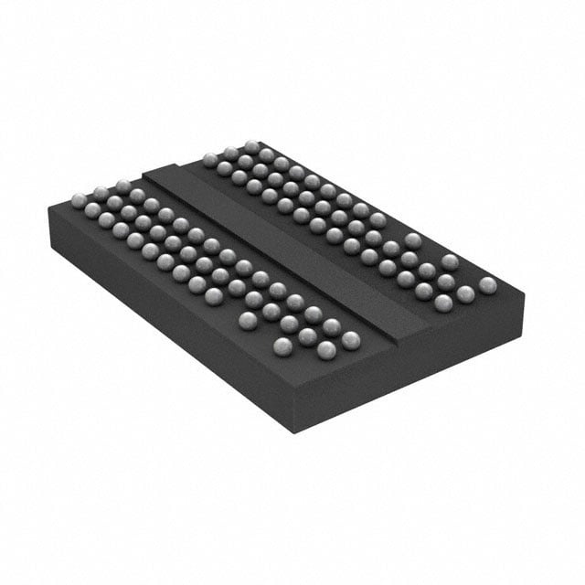
MT47H32M8BP-37E:B TR
| Part Description |
IC DRAM 256MBIT PAR 60FBGA |
|---|---|
| Quantity | 1,003 Available (as of June 15, 2026) |

| Product Category | Memory |
|---|---|
| Manufacturer | Micron Technology Inc. |
| Manufacturing Status | Obsolete |
| Manufacturer Standard Lead Time | Contact Us |
| Datasheet |
Specifications & Environmental
| Device Package | 60-FBGA (8x12) | Memory Format | DRAM | Technology | SDRAM - DDR2 | ||
|---|---|---|---|---|---|---|---|
| Memory Size | 256 Mbit | Access Time | 500 ps | Grade | Commercial (Extended) | ||
| Clock Frequency | 267 MHz | Voltage | 1.7V ~ 1.9V | Memory Type | Volatile | ||
| Operating Temperature | 0°C ~ 85°C (TC) | Write Cycle Time Word Page | 15 ns | Packaging | 60-FBGA | ||
| Mounting Method | Volatile | Memory Interface | Parallel | Memory Organization | 32M x 8 | ||
| Moisture Sensitivity Level | 3 (168 Hours) | RoHS Compliance | ROHS3 Compliant | REACH Compliance | REACH Unaffected | ||
| Qualification | N/A | ECCN | EAR99 | HTS Code | 8542.32.0024 |
Overview of MT47H32M8BP-37E:B TR – IC DRAM 256MBIT PAR 60FBGA
The MT47H32M8BP-37E:B TR is a 256 Mbit DDR2 SDRAM device organized as 32M × 8 with a parallel memory interface in a 60-ball FBGA (8 × 12 mm) package. It implements DDR2 architecture with a 4n-bit prefetch, 4 internal banks and features such as programmable CAS latency, DLL, and optional differential data strobe for robust synchronous operation.
This device is intended for designs requiring low-voltage DDR2 memory (VDD = 1.7 V–1.9 V / typical 1.8 V ±0.1 V) in a compact FBGA footprint and operating over a commercial temperature range of 0°C to 85°C. Key value propositions include flexible timing options, on-die termination and selectable burst lengths for system memory integration and signal integrity control.
Key Features
- Memory Type & Organization DDR2 SDRAM, 256 Mbit capacity organized as 32M × 8 with 4 internal banks for concurrent operation.
- Core Architecture 4n-bit prefetch architecture with DLL to align DQ and DQS transitions and support for posted CAS additive latency.
- Performance & Timing Clock frequency listed as 267 MHz with an access time of 500 ps and a write cycle time (word page) of 15 ns. The -37E speed grade corresponds to timing-cycle time 3.75 ns @ CL = 4 (DDR2-533).
- Interface & Signaling Parallel memory interface with JEDEC-standard 1.8 V I/O (SSTL_18-compatible), optional differential data strobe (DQS/DQS#) and duplicate output strobe (RDQS) option for x8 devices.
- Signal Integrity On-die termination (ODT), adjustable data-output drive strength and support for JEDEC clock jitter specification improve signal integrity on high-speed interfaces.
- Burst & Latency Options Programmable CAS latency, selectable burst lengths of 4 or 8, and WRITE latency defined as READ latency − 1 tCK.
- Refresh & Reliability 64 ms refresh interval implemented as 8,192-cycle refresh to maintain data retention in dynamic memory.
- Power Operates from 1.7 V to 1.9 V (typical 1.8 V ±0.1 V as documented in the datasheet).
- Package & Temperature 60-ball FBGA (8 mm × 12 mm) package; commercial operating temperature range 0°C to 85°C (TC).
- Compliance Datasheet lists RoHS compliant and support for JEDEC clock jitter specification.
Typical Applications
- Embedded Systems Compact 60-FBGA footprint and 1.8 V DDR2 signaling make this device suitable for embedded memory implementations where board space and low-voltage operation are important.
- Consumer Electronics Commercial-temperature-rated DDR2 SDRAM for consumer devices that require parallel DDR2 memory with programmable latency and selectable burst lengths.
- Network and Communications Equipment Parallel DDR2 memory with on-die termination, DLL and adjustable drive strength supports systems requiring controlled signal integrity on high-speed memory buses.
Unique Advantages
- Flexible Timing Configuration: Programmable CAS latency and selectable burst lengths (4 or 8) enable tuning for various memory access patterns and system timing requirements.
- Low-Voltage Operation: 1.7 V–1.9 V supply range (typical 1.8 V ±0.1 V) reduces power envelope while maintaining DDR2 signaling compatibility.
- Signal Integrity Features: On-die termination, DLL alignment of DQ/DQS, and adjustable drive strength help maintain reliable high-speed transfer in parallel memory systems.
- Compact Package: 60-ball FBGA (8 × 12 mm) provides a space-efficient footprint for dense board layouts.
- Predictable Refresh and Retention: 64 ms / 8,192-cycle refresh scheme provides standard DRAM retention behavior for system designers.
Why Choose MT47H32M8BP-37E:B TR?
The MT47H32M8BP-37E:B TR positions itself as a commercially rated DDR2 SDRAM option delivering 256 Mbit capacity in an x8 organization with flexible timing, on-die termination and DDR2 signaling at 1.8 V. Its combination of programmable latencies, DLL support and selectable burst lengths makes it appropriate for designs that need configurable memory timing and controlled signal integrity in a compact FBGA package.
This device is well suited for engineers and procurement teams specifying parallel DDR2 memory for commercial-temperature embedded, consumer or communications products where a 60-ball FBGA form factor, low-voltage operation and standard DRAM refresh behavior are required.
Request a quote or submit a product inquiry to receive pricing and availability information for the MT47H32M8BP-37E:B TR.