MT47H64M8CB-5E:B
| Part Description |
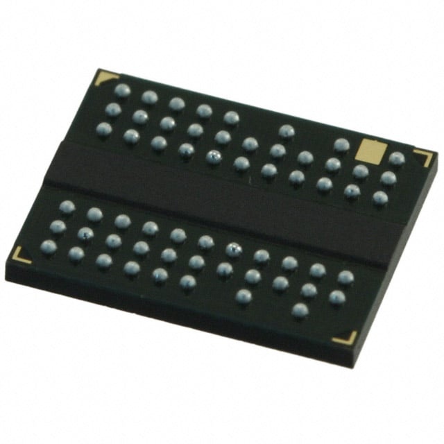
IC DRAM 512MBIT PARALLEL 60FBGA |
|---|---|
| Quantity | 337 Available (as of June 15, 2026) |
| Product Category | Memory |
|---|---|
| Manufacturer | Micron Technology Inc. |
| Manufacturing Status | Obsolete |
| Manufacturer Standard Lead Time | Contact Us |
| Datasheet |
Specifications & Environmental
| Device Package | 60-FBGA | Memory Format | DRAM | Technology | SDRAM - DDR2 | ||
|---|---|---|---|---|---|---|---|
| Memory Size | 512 Mbit | Access Time | 600 ps | Grade | Commercial (Extended) | ||
| Clock Frequency | 200 MHz | Voltage | 1.7V ~ 1.9V | Memory Type | Volatile | ||
| Operating Temperature | 0°C ~ 85°C (TC) | Write Cycle Time Word Page | 15 ns | Packaging | 60-FBGA | ||
| Mounting Method | Volatile | Memory Interface | Parallel | Memory Organization | 64M x 8 | ||
| Moisture Sensitivity Level | 5 (48 Hours) | RoHS Compliance | ROHS3 Compliant | REACH Compliance | REACH Unaffected | ||
| Qualification | N/A | ECCN | EAR99 | HTS Code | 8542.32.0024 |
Overview of MT47H64M8CB-5E:B – IC DRAM 512Mbit Parallel 60FBGA
The MT47H64M8CB-5E:B is a 512 Mbit DDR2 SDRAM organized as 64M × 8 in a 60-ball FBGA package. It implements a 4-bank DDR2 architecture with features from the device datasheet such as DLL alignment, selectable burst length, and programmable CAS latency.
This device targets designs that require parallel DDR2 memory with a 1.8 V supply range and commercial operating temperature, offering standard DDR2 signaling options and on-die termination to simplify high-speed interface design.
Key Features
- Core / Architecture DDR2 SDRAM with 4 internal banks and a 4n-bit prefetch architecture; DLL aligns DQ and DQS transitions with CK.
- Memory Organization 512 Mbit capacity arranged as 64M × 8 (16 Meg × 8 × 4 banks) suitable for parallel memory maps.
- Performance & Timing Specified clock frequency of 200 MHz, access time of 600 ps, and write cycle time (word page) of 15 ns; programmable CAS latency and posted CAS additive latency are supported.
- Data Interface JEDEC-standard 1.8 V I/O (SSTL_18-compatible) with options for differential data strobe (DQS/DQS#) and duplicate output strobe (RDQS) for x8 devices.
- Power Vdd and VddQ specified at +1.8 V ±0.1 V (1.7 V – 1.9 V supply range).
- Signal Integrity On-die termination (ODT) and adjustable data-output drive strength to assist in meeting system timing and signal integrity requirements.
- Refresh & Reliability 8,192-cycle (8K) refresh count and 64 ms refresh interval as defined in the datasheet.
- Package 60-ball FBGA (60-FBGA) supplier device package; compact footprint for board integration.
- Operating Temperature Commercial temperature range: 0°C to 85°C (T_C).
- Standards & Options Supports JEDEC clock jitter specifications; datasheet lists selectable timing grades and options including RoHS compliant and various package/revision markings.
Typical Applications
- Embedded memory subsystems Use as on-board parallel DDR2 DRAM where 512 Mbit capacity and 60-FBGA packaging meet form-factor and interface requirements.
- Consumer and portable electronics Fits devices requiring DDR2 memory at 1.8 V supply and commercial temperature range with selectable CAS and burst settings.
- Networking and communications modules Provides parallel DDR2 buffering and working memory for systems that need 4-bank concurrent operation and adjustable drive strength.
- Industrial control equipment (commercial-temp) Applicable for systems operating within 0°C to 85°C that require DDR2 memory with on-die termination and JEDEC-compliant signaling.
Unique Advantages
- Standard DDR2 signaling: JEDEC-standard 1.8 V I/O (SSTL_18-compatible) simplifies integration with common DDR2 interfaces.
- Flexible timing configuration: Programmable CAS latency and posted additive latency allow designers to tune performance to system timing and throughput needs.
- Integrated signal management: DLL alignment, on-die termination, and adjustable drive strength help address timing alignment and signal integrity challenges at DDR2 speeds.
- Compact FBGA package: 60-ball FBGA provides a small footprint for space-constrained boards while maintaining a parallel memory interface.
- Power-optimized DDR2 supply: Operation at Vdd/VddQ = 1.8 V ±0.1 V supports lower-voltage system designs that follow DDR2 power rails.
Why Choose MT47H64M8CB-5E:B?
The MT47H64M8CB-5E:B delivers a standards-based DDR2 SDRAM solution in a compact 60-FBGA package with 512 Mbit capacity and a 64M × 8 organization. Its combination of programmable timing, DLL alignment, on-die termination, and adjustable drive strength provides the control engineers need to meet system timing and signal integrity targets.
This device is suited for developers and procurement teams specifying parallel DDR2 memory for commercial-temperature systems that require JEDEC-compliant signaling, 1.8 V operation, and selectable performance options defined in the datasheet.
Request a quote or submit an inquiry to our sales team to discuss pricing, availability, and device options for the MT47H64M8CB-5E:B.