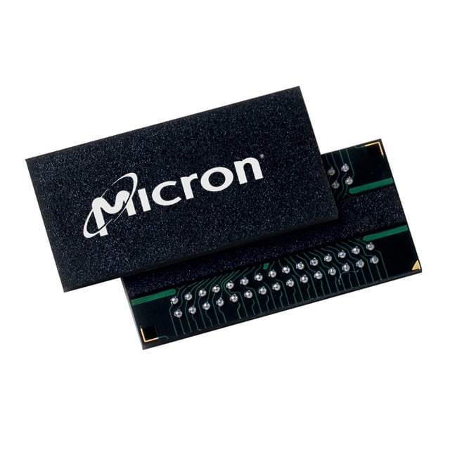
MT47H64M8CF-25E IT:G
| Part Description |
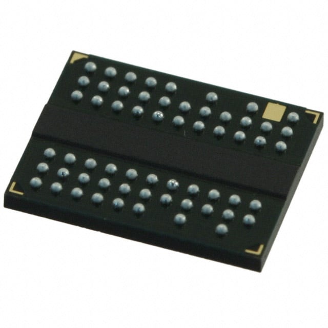
IC DRAM 512MBIT PARALLEL 60FBGA |
|---|---|
| Quantity | 66 Available (as of June 18, 2026) |

| Product Category | DRAM Memory |
|---|---|
| Manufacturer | Micron Technology Inc. |
| Manufacturing Status | Obsolete |
| Manufacturer Standard Lead Time | Contact Us |
| Datasheet |
Specifications & Environmental
| Device Package | 60-FBGA (8x10) | Memory Format | DRAM | Technology | SDRAM - DDR2 | ||
|---|---|---|---|---|---|---|---|
| Memory Size | 512 Mbit | Access Time | 400 ps | Grade | Automotive | ||
| Clock Frequency | 400 MHz | Voltage | 1.7V ~ 1.9V | Memory Type | Volatile | ||
| Operating Temperature | -40°C ~ 95°C (TC) | Write Cycle Time Word Page | 15 ns | Packaging | 60-TFBGA | ||
| Mounting Method | Volatile | Memory Interface | Parallel | Memory Organization | 64M x 8 | ||
| Moisture Sensitivity Level | 3 (168 Hours) | RoHS Compliance | ROHS3 Compliant | REACH Compliance | REACH Unaffected | ||
| Qualification | N/A | ECCN | EAR99 | HTS Code | 8542.32.0028 |
Overview of MT47H64M8CF-25E IT:G – IC DRAM 512MBIT PARALLEL 60FBGA
The MT47H64M8CF-25E IT:G is a 512Mbit DDR2 SDRAM organized as 64M × 8 with a parallel memory interface in a 60-ball TFBGA package. It implements DDR2 architecture with a 4n-bit prefetch, DLL alignment, and selectable burst lengths to support standard synchronous memory operations.
Targeted at industrial-temperature systems, this device delivers 400 MHz clock operation (DDR2-800 timing options), JEDEC-standard 1.8 V I/O, and on-die termination features that simplify integration in embedded and industrial designs requiring a compact FBGA footprint and low-voltage operation.
Key Features
- Memory Core and Organization 512 Mbit DDR2 SDRAM organized as 64M × 8 with 4 internal banks and a 4n-bit prefetch architecture.
- Performance / Timing Supports clock rates up to 400 MHz (DDR2 data rates per listed speed grades) with programmable CAS latency, posted CAS additive latency, and selectable burst lengths of 4 or 8.
- Data Path and Signaling JEDEC-standard 1.8 V I/O (SSTL_18-compatible) with options for differential data strobe (DQS/DQS#) and duplicate output strobe (RDQS) for x8 devices; DLL aligns DQ and DQS transitions with CK.
- Power and Voltage Core and I/O operate at VDD = VDDQ = 1.8 V ± 0.1 V (product specified supply range 1.7 V to 1.9 V).
- Signal Integrity and Drive On-die termination (ODT) and adjustable data-output drive strength to help optimize board-level signal integrity.
- Refresh and Reliability Standard 8k refresh count with 64 ms refresh interval and support for self-refresh options.
- Package and Mounting 60-TFBGA (60-ball FBGA, 8 mm × 10 mm) supplier device package; surface-mount FBGA footprint for compact board-level integration.
- Temperature Range Industrial temperature option with device operating range shown as −40 °C to 95 °C (TC).
- Additional DDR2 Features Duplicate output strobe option for x8, programmable write/read latency relationship, and support for JEDEC clock jitter specifications.
Typical Applications
- Industrial Embedded Systems — Memory for embedded controllers and industrial platforms that require operation across an extended temperature range (−40 °C to 95 °C).
- Legacy DDR2 Platforms — System upgrades or designs that use DDR2 SDRAM with JEDEC-standard 1.8 V I/O and parallel memory interfaces.
- Compact Board-Level Designs — Applications needing a 512 Mbit DDR2 device in a 60-ball FBGA package for reduced PCB footprint.
- Parallel-Interface Memory Expansion — Designs requiring a standard x8 memory organization (64M × 8) with selectable burst and timing options for predictable integration.
Unique Advantages
- Industry-Standard DDR2 Interface: JEDEC-compatible DDR2 signaling and programmable timing simplify integration into existing DDR2 memory subsystems.
- Extended Temperature Support: Industrial temperature option enables deployment in environments from −40 °C to 95 °C for ruggedized applications.
- Low-Voltage Operation: 1.8 V core and I/O operation (1.7 V to 1.9 V supply range) reduces system power budget relative to higher-voltage alternatives.
- On-Die Termination and Drive Control: ODT and adjustable output drive strength help manage signal integrity on high-speed DDR2 buses.
- Compact FBGA Package: 60-ball FBGA (8 mm × 10 mm) provides a small-footprint mounting option for space-constrained PCBs.
Why Choose MT47H64M8CF-25E IT:G?
The MT47H64M8CF-25E IT:G combines standard-compliant DDR2 features with a 512 Mbit density in a compact 60-ball FBGA package, making it suitable for industrial and embedded designs that require reliable, parallel DDR2 memory. Its programmable timing, ODT, and JEDEC-standard signaling allow predictable integration into systems using DDR2 memory interfaces.
Manufactured by Micron Technology, Inc., this part aligns with common DDR2 refresh and timing architectures and is offered with industrial temperature capability for applications that must operate across extended thermal environments.
Request a quote or submit a pricing inquiry to receive availability and lead-time information for the MT47H64M8CF-25E IT:G.