MT47H64M8CF-25E L:G
| Part Description |
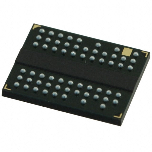
IC DRAM 512MBIT PARALLEL 60FBGA |
|---|---|
| Quantity | 1,647 Available (as of June 14, 2026) |

| Product Category | Memory |
|---|---|
| Manufacturer | Micron Technology Inc. |
| Manufacturing Status | Obsolete |
| Manufacturer Standard Lead Time | Contact Us |
| Datasheet |
Specifications & Environmental
| Device Package | 60-FBGA (8x10) | Memory Format | DRAM | Technology | SDRAM - DDR2 | ||
|---|---|---|---|---|---|---|---|
| Memory Size | 512 Mbit | Access Time | 400 ps | Grade | Commercial (Extended) | ||
| Clock Frequency | 400 MHz | Voltage | 1.7V ~ 1.9V | Memory Type | Volatile | ||
| Operating Temperature | 0°C ~ 85°C (TC) | Write Cycle Time Word Page | 15 ns | Packaging | 60-TFBGA | ||
| Mounting Method | Volatile | Memory Interface | Parallel | Memory Organization | 64M x 8 | ||
| Moisture Sensitivity Level | 3 (168 Hours) | RoHS Compliance | ROHS3 Compliant | REACH Compliance | REACH Unaffected | ||
| Qualification | N/A | ECCN | EAR99 | HTS Code | 8542.32.0028 |
Overview of MT47H64M8CF-25E L:G – IC DRAM 512MBIT PARALLEL 60FBGA
The MT47H64M8CF-25E L:G is a 512 Mbit DDR2 SDRAM organized as 64M × 8 with a parallel memory interface in a 60-ball FBGA package. It implements a 4-bank DDR2 architecture with JEDEC-standard 1.8 V I/O and is specified for commercial temperature operation (0°C to 85°C).
Designed for systems requiring compact DDR2 volatile memory, the device offers 400 MHz clock operation, fast access timing, and platform-level features such as on-die termination and programmable timing options to support a range of DDR2-based designs.
Key Features
- Memory Core 512 Mbit DDR2 SDRAM organized as 64M × 8 with four internal banks for concurrent operation.
- Performance Clock frequency specified at 400 MHz with an access time of 400 ps and timing options including programmable CAS latency and posted CAS additive latency.
- DDR2 Architecture 4n-bit prefetch architecture, DLL to align DQ and DQS with CK, and selectable burst lengths of 4 or 8 to support typical DDR2 access patterns.
- Data Strobe and Output Options Differential data strobe (DQS/DQS#) option; duplicate output strobe (RDQS) option available for x8 configuration.
- Signal Integrity and Drive JEDEC-standard 1.8 V I/O (SSTL_18-compatible) with adjustable data-output drive strength and on-die termination (ODT) to simplify board-level termination.
- Power and Voltage Supply voltage range listed as 1.7 V to 1.9 V (nominal +1.8 V ±0.1 V for VDD and VDDQ).
- Refresh and Reliability Features 64 ms, 8192-cycle refresh support to meet standard DRAM maintenance requirements.
- Package and Temperature 60-ball TFBGA (8 mm × 10 mm) package with commercial operating temperature range 0°C to 85°C.
Typical Applications
- Memory expansion for DDR2 platforms — Provides a compact 512 Mbit DDR2 option for systems requiring standard parallel DDR2 memory.
- Embedded systems — Compact 60-ball FBGA package and 1.8 V I/O suited to space-constrained board designs that implement DDR2 memory.
- Platform-level buffering and frame storage — 4-bank DDR2 architecture and selectable burst lengths support common buffering use cases in digital systems.
Unique Advantages
- JEDEC-standard 1.8 V I/O: Ensures compatibility with standard DDR2 signaling (SSTL_18-compatible) for straightforward interface design.
- Compact FBGA package: 60-ball (8×10 mm) TFBGA footprint reduces board area while providing standard FBGA mounting.
- Flexible timing and drive control: Programmable CAS latency, additive latency, and adjustable output drive strength allow tuning for system timing and signal integrity.
- On-die termination and DLL: Integrated ODT and DLL reduce external termination complexity and help align data strobes for reliable high-speed operation.
- Commercial temperature rating: Specified 0°C to 85°C operation for designs targeting standard commercial environments.
Why Choose IC DRAM 512MBIT PARALLEL 60FBGA?
The MT47H64M8CF-25E L:G delivers a verified DDR2 SDRAM building block with 512 Mbit capacity, a 64M × 8 organization, and a compact 60-ball FBGA package for systems that require a standard 1.8 V DDR2 memory solution. Its combination of programmable timing, on-die termination, and data-strobe options supports designers focused on reliable high-speed parallel memory interfaces.
This device is well suited to engineers and procurement teams specifying commercial-temperature DDR2 memory for embedded and platform designs where compact packaging, standard JEDEC signaling, and configurable timing/drive behavior are important for integration and signal integrity control.
Request a quote or contact sales to discuss availability, lead times, and volume pricing for the MT47H64M8CF-25E L:G.