MT47H64M8CF-25E:G TR
| Part Description |
IC DRAM 512MBIT PARALLEL 60FBGA |
|---|---|
| Quantity | 597 Available (as of June 15, 2026) |
| Product Category | Memory |
|---|---|
| Manufacturer | Micron Technology Inc. |
| Manufacturing Status | Obsolete |
| Manufacturer Standard Lead Time | Contact Us |
| Datasheet |
Specifications & Environmental
| Device Package | 60-FBGA (8x10) | Memory Format | DRAM | Technology | SDRAM - DDR2 | ||
|---|---|---|---|---|---|---|---|
| Memory Size | 512 Mbit | Access Time | 400 ps | Grade | Commercial (Extended) | ||
| Clock Frequency | 400 MHz | Voltage | 1.7V ~ 1.9V | Memory Type | Volatile | ||
| Operating Temperature | 0°C ~ 85°C (TC) | Write Cycle Time Word Page | 15 ns | Packaging | 60-TFBGA | ||
| Mounting Method | Volatile | Memory Interface | Parallel | Memory Organization | 64M x 8 | ||
| Moisture Sensitivity Level | 3 (168 Hours) | RoHS Compliance | ROHS3 Compliant | REACH Compliance | REACH Unaffected | ||
| Qualification | N/A | ECCN | EAR99 | HTS Code | 8542.32.0024 |
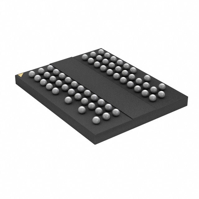
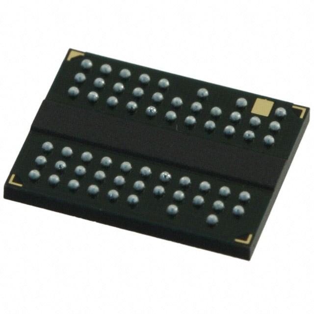
Overview of MT47H64M8CF-25E:G TR – IC DRAM 512MBIT PARALLEL 60FBGA
The MT47H64M8CF-25E:G TR is a 512 Mbit DDR2 SDRAM organized as 64M × 8 with a parallel memory interface in a 60-ball TFBGA package (8 mm × 10 mm). It implements DDR2 architecture with a 4n-bit prefetch and supports standard DDR2 timing and control features.
Designed for systems requiring JEDEC-standard 1.8 V I/O operation and commercial temperature operation (0°C to 85°C), this device offers programmable timing, on-die termination and options for differential data strobe to support reliable high-speed data transfers at DDR2 rates.
Key Features
- Core / Memory Architecture — 512 Mbit DDR2 SDRAM organized as 64M × 8 with 4 internal banks for concurrent operation (16M × 8 × 4 banks).
- Performance & Timing — Supports DDR2 timing including programmable CAS latency and selectable burst lengths of 4 or 8; specified clock frequency 400 MHz and access time 400 ps. Write cycle time (word page) is 15 ns.
- Power & I/O — VDD / VDDQ supply range 1.7 V to 1.9 V (JEDEC-standard 1.8 V ±0.1 V) with adjustable data-output drive strength and SSTL_18-compatible I/O.
- Signal Integrity & Timing Control — DLL aligns DQ and DQS transitions with CK; on-die termination (ODT) and differential data strobe (DQS/DQS#) option improve signal timing and integrity. Duplicate output strobe (RDQS) option available for x8 configuration.
- Refresh & Reliability — Standard 64 ms, 8192-cycle refresh; supports JEDEC clock jitter specification for stable operation at specified DDR2 data rates. Datasheet documents industrial and automotive package options, while this part is specified for commercial temperature range.
- Package — 60-ball FBGA (8 mm × 10 mm, TFBGA) compact supplier device package for surface-mount applications.
- Compliance — Datasheet lists RoHS-compliant options for the family.
Typical Applications
- Legacy DDR2 system memory — Provides 512 Mbit DDR2 storage for platforms and designs built around parallel DDR2 SDRAM interfaces operating at commercial temperatures.
- Embedded memory subsystems — Compact 60-ball FBGA package suits space-constrained boards that require standard 1.8 V DDR2 memory with programmable timing.
- Consumer and industrial electronics — Commercial-temperature designs that need DDR2 performance with on-die termination and burst-mode transfers benefit from this device’s features.
Unique Advantages
- JEDEC-standard 1.8 V I/O: Ensures compatibility with SSTL_18 signaling and standard DDR2 host interfaces.
- Flexible timing and burst control: Programmable CAS latency and selectable burst lengths (4 or 8) allow designers to tune performance for specific system timing requirements.
- Signal integrity features: On-die termination, DLL alignment of DQ/DQS, and differential DQS options reduce design margin risk at DDR2 data rates.
- Compact BGA footprint: 60-ball TFBGA (8 mm × 10 mm) minimizes board area while providing a full DDR2 64M × 8 organization.
- Commercial temperature rating: Specified 0°C to 85°C operation for mainstream consumer and many industrial applications.
Why Choose IC DRAM 512MBIT PARALLEL 60FBGA?
The MT47H64M8CF-25E:G TR delivers a straightforward, standards-based DDR2 memory solution with 512 Mbit density, JEDEC 1.8 V I/O compatibility, and on-die features that simplify signal integrity and timing design. Its 64M × 8 organization, programmable timing, and selectable burst lengths make it suitable for designs that require deterministic DDR2 behavior in a compact FBGA package.
This part is targeted at designers and procurement teams implementing commercial-temperature DDR2 memory subsystems who need a documented, standards-aligned DRAM device with configurable timing and integrated signal-management features to support reliable operation at specified DDR2 data rates.
Request a quote or submit an inquiry for pricing and availability to receive further purchasing and lead-time information.