MT47H64M8SH-25E AAT:H TR
| Part Description |
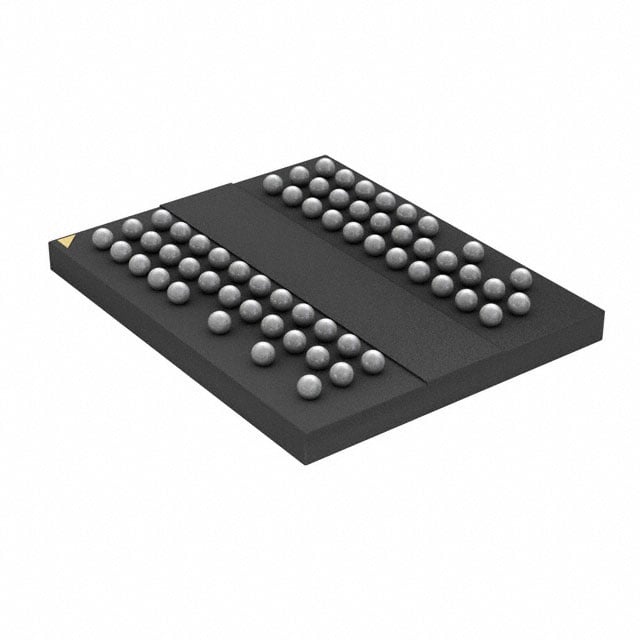
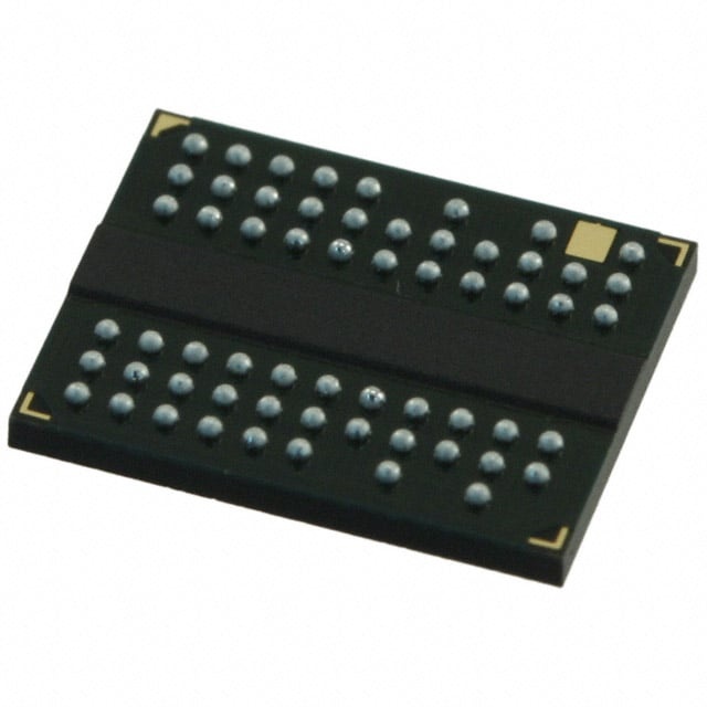
IC DRAM 512MBIT PARALLEL 60FBGA |
|---|---|
| Quantity | 864 Available (as of June 15, 2026) |

| Product Category | Memory |
|---|---|
| Manufacturer | Micron Technology Inc. |
| Manufacturing Status | Obsolete |
| Manufacturer Standard Lead Time | Contact Us |
| Datasheet |
Specifications & Environmental
| Device Package | 60-FBGA (8x10) | Memory Format | DRAM | Technology | SDRAM - DDR2 | ||
|---|---|---|---|---|---|---|---|
| Memory Size | 512 Mbit | Access Time | 400 ps | Grade | Automotive | ||
| Clock Frequency | 400 MHz | Voltage | 1.7V ~ 1.9V | Memory Type | Volatile | ||
| Operating Temperature | -40°C ~ 105°C (TA) | Write Cycle Time Word Page | 15 ns | Packaging | 60-TFBGA | ||
| Mounting Method | Volatile | Memory Interface | Parallel | Memory Organization | 64M x 8 | ||
| Moisture Sensitivity Level | 3 (168 Hours) | RoHS Compliance | ROHS3 Compliant | REACH Compliance | REACH Unaffected | ||
| Qualification | AEC-Q100 | ECCN | EAR99 | HTS Code | 8542.32.0032 |
Overview of MT47H64M8SH-25E AAT:H TR – IC DRAM 512Mbit Parallel 60‑FBGA
The MT47H64M8SH-25E AAT:H TR is a 512 Mbit DDR2 SDRAM organized as 64M × 8 with a parallel memory interface, designed for demanding embedded applications. It implements a 4‑bank DDR2 architecture with features such as DLL alignment, on‑die termination and selectable burst lengths to support high‑speed data transfers.
Targeted at automotive and industrial markets, this device offers automotive qualification (AEC‑Q100) and an extended ambient operating range, providing a compact, low‑voltage 1.8 V solution in a 60‑ball TFBGA (8 × 10 mm) package.
Key Features
- Memory Core 512 Mbit DDR2 SDRAM organized as 64M × 8 with 4 internal banks and 4n‑bit prefetch architecture for concurrent memory operations.
- Performance & Timing Clock frequency up to 400 MHz (DDR2 data rates supported); write cycle time (word page) of 15 ns and access time of 400 ps. Programmable CAS latency and selectable burst lengths (4 or 8).
- Data Interface & Signal Integrity JEDEC‑standard 1.8 V I/O (SSTL_18‑compatible), DLL to align DQ and DQS, optional differential data strobe (DQS/DQS#) and duplicate RDQS option for x8 configurations; on‑die termination (ODT) supported.
- Power Nominal supply VDD/VDDQ = 1.8 V with operating range 1.7 V to 1.9 V to support low‑voltage system designs.
- Reliability & Automotive AEC‑Q100 qualification, PPAP submission and 8D response time noted in documentation; supports JEDEC clock jitter specification and RoHS compliance.
- Package & Temperature 60‑TFBGA (60‑ball FBGA, 8 × 10 mm) package; ambient operating range −40 °C to +105 °C (TA) suitable for extended temperature applications.
- Refresh & System 8192‑cycle refresh with 64 ms refresh interval and features (programmable CL, additive latency, WRITE latency behavior) to support typical DDR2 system timing requirements.
Typical Applications
- Automotive systems — Suitable for automotive electronic modules requiring automotive‑qualified DDR2 memory in extended temperature environments.
- Telematics and infotainment — Provides parallel DDR2 memory capacity for data buffering and media applications in embedded in‑vehicle systems.
- Industrial and ruggedized equipment — Low‑voltage, wide temperature operation and AEC‑Q100 qualification make it applicable where environmental robustness is required.
- Embedded controllers and processors — Serves as external DRAM for embedded platforms that require a compact FBGA memory footprint and DDR2 performance.
Unique Advantages
- Automotive‑qualified reliability: AEC‑Q100 qualification and −40 °C to +105 °C ambient rating enable use in automotive and other harsh environments.
- Compact FBGA package: 60‑ball TFBGA (8 × 10 mm) minimizes PCB area while providing a full DDR2 parallel interface.
- Low‑voltage operation: 1.7 V to 1.9 V supply range (nominal 1.8 V) supports energy‑efficient system designs.
- DDR2 timing flexibility: Programmable CAS latency, DLL alignment, selectable burst lengths and standard DDR2 timing options allow tuning for system performance and compatibility.
- Signal integrity features: On‑die termination, differential DQS options and adjustable data‑output drive strength help simplify high‑speed board design and routing.
- Documentation and quality process notes: Device documentation lists PPAP submission and 8D response capability, supporting automotive production and quality workflows.
Why Choose IC DRAM 512MBIT PARALLEL 60FBGA?
The MT47H64M8SH-25E AAT:H TR delivers a compact 512 Mbit DDR2 memory solution with automotive qualification and robust signal‑integrity features tailored for embedded and vehicle applications. Its combination of low‑voltage operation, programmable timing and FBGA packaging makes it suitable for designers seeking a verified DDR2 memory building block for temperature‑challenging environments.
Use this device in designs that require a verified automotive‑grade DDR2 memory component with documentation for production quality processes and the timing flexibility to integrate with a range of DDR2 controller implementations.
Request a quote or submit an inquiry for pricing and availability to evaluate the MT47H64M8SH-25E AAT:H TR for your next design.