MT48LC4M16A2TG-6:G
| Part Description |
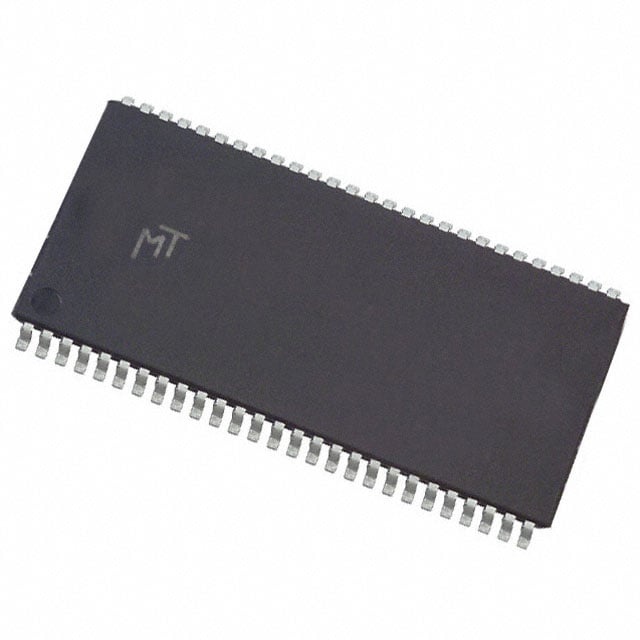
IC DRAM 64MBIT PAR 54TSOP II |
|---|---|
| Quantity | 657 Available (as of June 11, 2026) |

| Product Category | Memory |
|---|---|
| Manufacturer | Micron Technology Inc. |
| Manufacturing Status | Obsolete |
| Manufacturer Standard Lead Time | Contact Us |
| Datasheet |
Specifications & Environmental
| Device Package | 54-TSOP II | Memory Format | DRAM | Technology | SDRAM | ||
|---|---|---|---|---|---|---|---|
| Memory Size | 64 Mbit | Access Time | 5.5 ns | Grade | Commercial | ||
| Clock Frequency | 167 MHz | Voltage | 3V ~ 3.6V | Memory Type | Volatile | ||
| Operating Temperature | 0°C ~ 70°C (TA) | Write Cycle Time Word Page | 12 ns | Packaging | 54-TSOP (0.400", 10.16mm Width) | ||
| Mounting Method | Volatile | Memory Interface | Parallel | Memory Organization | 4M x 16 | ||
| Moisture Sensitivity Level | 2 (1 Year) | RoHS Compliance | N/A | REACH Compliance | REACH Unaffected | ||
| Qualification | N/A | ECCN | EAR99 | HTS Code | 8542.32.0002 |
Overview of MT48LC4M16A2TG-6:G – IC DRAM 64MBIT PAR 54TSOP II
The MT48LC4M16A2TG-6:G is a 64 Mbit synchronous DRAM (SDRAM) organized as 4M × 16 with a parallel memory interface in a 54-pin TSOP II (0.400", 10.16 mm width) package. It operates from a single 3.3 V supply range and is specified for commercial ambient temperatures (0 °C to +70 °C).
Designed for systems that require synchronous, pipelined DRAM operation, it supports programmable burst lengths, internal bank management and standard/self refresh modes. Note: the datasheet includes a notation that this device is not recommended for new designs.
Key Features
- Core & Architecture Fully synchronous SDRAM with internal pipelined operation and internal banks for hiding row access/precharge, enabling column address changes every clock cycle.
- Memory Organization 64 Mbit capacity configured as 4M × 16 with four internal banks.
- Performance & Timing Supports up to 167 MHz clock frequency with an access time of 5.5 ns and a write cycle time (word/page) of 12 ns; programmable CAS and burst operation.
- Refresh & Power Modes Auto Refresh and Auto Precharge modes, plus standard and low-power Self Refresh; 64 ms / 4,096-cycle refresh supported.
- Voltage & I/O Single supply operation at 3.3 V nominal (3.0 V to 3.6 V range) with LVTTL-compatible inputs and outputs.
- Package & Temperature 54-pin TSOP II (400 mil) plastic package, 10.16 mm width; commercial operating temperature range 0 °C to +70 °C.
- Standards Compatibility Documented PC66-, PC100- and PC133-compliant timing options in the datasheet.
Typical Applications
- PC memory subsystems — Suitable for designs that require PC66/PC100/PC133-compliant synchronous DRAM timing.
- Embedded and commercial systems — Works in systems running from a 3.3 V supply with a commercial 0 °C to +70 °C ambient range where parallel SDRAM is specified.
- Parallel SDRAM modules and buffers — Used where a compact 54-pin TSOP II package and a 4M × 16 organization are appropriate for board-level memory implementations.
Unique Advantages
- Synchronous pipelined operation: Enables column address changes every clock cycle for predictable, clocked memory behavior.
- Flexible burst control: Programmable burst lengths (1, 2, 4, 8 or full page) to match different data-transfer patterns.
- Integrated refresh management: Auto Refresh and Self Refresh modes reduce external refresh handling and support low-power retention modes.
- Single-supply LVTTL I/O: Operates from a single +3.3 V supply with LVTTL-compatible inputs/outputs for straightforward interfacing.
- Compact board footprint: 54-pin TSOP II (400 mil) package provides a small profile for space-constrained designs.
- Vendor-specified timing options: Datasheet lists PC66/PC100/PC133 timing variants to support established synchronous memory timing families.
Why Choose MT48LC4M16A2TG-6:G?
The MT48LC4M16A2TG-6:G offers a documented SDRAM solution with a 4M × 16 organization, supported timing variants and standard refresh/power modes, packaged in a compact 54-pin TSOP II. Its single 3.3 V supply, LVTTL I/O compatibility and commercial temperature rating make it suitable for existing designs and modules that require synchronous parallel DRAM behavior.
Because the datasheet specifies compliance with PC66/PC100/PC133 timing options and provides detailed timing and refresh characteristics, this device is well suited for engineers maintaining or supporting systems that rely on these synchronous DRAM conventions. Refer to the device datasheet notes for lifecycle considerations.
To request a quote or for availability and lead-time information, please contact sales or submit a quote request through your preferred procurement channel.