MT48LC4M16A2TG-75:G TR
| Part Description |
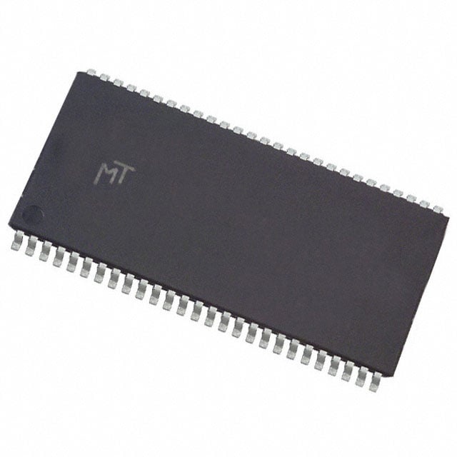
IC DRAM 64MBIT PAR 54TSOP II |
|---|---|
| Quantity | 792 Available (as of June 15, 2026) |

| Product Category | Memory |
|---|---|
| Manufacturer | Micron Technology Inc. |
| Manufacturing Status | Obsolete |
| Manufacturer Standard Lead Time | Contact Us |
| Datasheet |
Specifications & Environmental
| Device Package | 54-TSOP II | Memory Format | DRAM | Technology | SDRAM | ||
|---|---|---|---|---|---|---|---|
| Memory Size | 64 Mbit | Access Time | 5.4 ns | Grade | Commercial | ||
| Clock Frequency | 133 MHz | Voltage | 3V ~ 3.6V | Memory Type | Volatile | ||
| Operating Temperature | 0°C ~ 70°C (TA) | Write Cycle Time Word Page | 15 ns | Packaging | 54-TSOP (0.400", 10.16mm Width) | ||
| Mounting Method | Volatile | Memory Interface | Parallel | Memory Organization | 4M x 16 | ||
| Moisture Sensitivity Level | 3 (168 Hours) | RoHS Compliance | RoHS non-compliant | REACH Compliance | REACH Unaffected | ||
| Qualification | N/A | ECCN | EAR99 | HTS Code | 8542.32.0002 |
Overview of MT48LC4M16A2TG-75:G TR – IC DRAM 64Mbit PAR 54TSOP II
The MT48LC4M16A2TG-75:G TR is a 64 Mbit synchronous DRAM organized as 4M × 16 with a parallel SDRAM interface in a 54-pin TSOP II package. It implements fully synchronous operation with internal pipelining and banked architecture to support high-throughput, low-latency memory access patterns.
Designed for systems requiring PC133‑class SDRAM performance, this device operates from a 3.0 V to 3.6 V supply, supports programmable burst lengths and auto/self‑refresh modes, and is offered in a compact 54‑pin TSOP II (400 mil, 10.16 mm width) package for board-level integration at commercial temperature ranges.
Key Features
- Memory Core 64 Mbit SDRAM organized as 1M × 16 × 4 banks (4M × 16 logical organization) for parallel data transfers.
- Performance PC66/PC100/PC133‑compliant timing options with a listed clock frequency of 133 MHz and an access time entry of 5.4 ns; the -75 timing option corresponds to a 7.5 ns cycle time at CL = 3 per datasheet timing options.
- Internal Architecture Fully synchronous operation with internal pipelined operation, internal banks for hiding row access/precharge, and the ability to change column address every clock cycle.
- Burst & Refresh Programmable burst lengths (1, 2, 4, 8, or full page), Auto Precharge (including concurrent Auto Precharge), Auto Refresh modes, and a 64 ms / 4,096‑cycle refresh scheme.
- Interface & I/O Parallel SDRAM interface with LVTTL‑compatible inputs and outputs and support for conventional DRAM control signals (CLK, CKE, CS#, BA0/BA1, A0–A11, DQ, DQM).
- Power Single‑supply operation at +3.3 V nominal (specified 3.0 V to 3.6 V) and standard/low power self‑refresh options documented in the datasheet.
- Package & Temperature 54‑pin TSOP II (400 mil, 10.16 mm width) plastic package; commercial operating temperature range 0 °C to +70 °C.
Typical Applications
- PC133‑class memory subsystems Systems requiring PC133‑compliant synchronous DRAM timing and parallel SDRAM interfaces.
- 3.3 V system memory Designs that operate from a 3.0 V to 3.6 V supply and require a 64 Mbit parallel DRAM device.
- Board‑level module integration PCB designs that need a compact 54‑pin TSOP II (400 mil) memory package for space-constrained layouts.
Unique Advantages
- PC133‑class timing options: Provides established timing selections including the -75 option (7.5 ns cycle at CL = 3) for compatibility with PC133 timing requirements.
- Flexible burst operation: Programmable burst lengths (1, 2, 4, 8, full page) enable tuning data transfer granularity to system access patterns.
- Banked, pipelined architecture: Internal banks and pipelined operation allow column address changes every clock cycle, improving effective throughput for sequential accesses.
- Comprehensive refresh and power modes: Auto Refresh, Auto Precharge (including concurrent Auto Precharge), and self‑refresh modes support data integrity with system power management.
- Compact, industry standard package: 54‑pin TSOP II (400 mil) package facilitates integration into existing board designs that require standard TSOP form factors.
- Vendor documentation: Detailed datasheet specifications and timing options are provided for design and timing validation.
Why Choose MT48LC4M16A2TG-75:G TR?
The MT48LC4M16A2TG-75:G TR offers a documented, PC133‑class synchronous DRAM solution in a 64 Mbit density with a parallel interface and a compact 54‑pin TSOP II package. Its banked, pipelined architecture, programmable burst modes, and standard power/refresh features make it suitable for designs that require established SDRAM timing and predictable board‑level integration.
This device is appropriate for designers and procurement teams specifying 3.3 V SDRAM memory at commercial temperature ranges who need clear datasheet guidance and defined timing options for system timing validation and layout implementation.
Request a quote or submit a sales inquiry to receive pricing, availability, and ordering information for the MT48LC4M16A2TG-75:G TR.