MT53E1G32D2FW-046 IT:B TR
| Part Description |
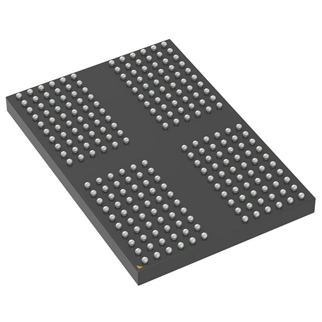
IC DRAM 32GBIT PAR 200TFBGA |
|---|---|
| Quantity | 1,527 Available (as of June 14, 2026) |

| Product Category | Memory |
|---|---|
| Manufacturer | Micron Technology Inc. |
| Manufacturing Status | Active |
| Manufacturer Standard Lead Time | 4 Weeks |
| Datasheet |
Specifications & Environmental
| Device Package | 200-TFBGA (10x14.5) | Memory Format | DRAM | Technology | SDRAM - Mobile LPDDR4X | ||
|---|---|---|---|---|---|---|---|
| Memory Size | 32 Gbit | Access Time | 3.5 ns | Grade | Automotive | ||
| Clock Frequency | 2.133 GHz | Voltage | 1.06V ~ 1.17V | Memory Type | Volatile | ||
| Operating Temperature | -40°C ~ 95°C (TC) | Write Cycle Time Word Page | 18 ns | Packaging | 200-TFBGA | ||
| Mounting Method | Volatile | Memory Interface | Parallel | Memory Organization | 1G x 32 | ||
| Moisture Sensitivity Level | 3 (168 Hours) | RoHS Compliance | ROHS3 Compliant | REACH Compliance | REACH Unaffected | ||
| Qualification | N/A | ECCN | EAR99 | HTS Code | 8542.32.0036 |
Overview of MT53E1G32D2FW-046 IT:B TR – 32Gbit LPDDR4X SDRAM, 200-TFBGA
The MT53E1G32D2FW-046 IT:B TR is a 32 Gbit LPDDR4/LPDDR4X parallel DRAM in a 200-TFBGA package configured as 1G × 32. It implements mobile LPDDR4X architecture with a high data rate interface and options for low-voltage VDDQ operation.
Designed for bandwidth‑intensive embedded and automotive-grade applications, this device delivers multi‑GHz clocking, low-voltage operation and package-level options that support compact board integration and extended temperature operation.
Key Features
- Memory Architecture — 1G × 32 organization providing 32 Gbit density in a parallel LPDDR4/LPDDR4X die configuration.
- High Data Rate — Supports 2133 MHz clock (data rate 4266 Mb/s per pin) enabling up to 8.5 GB/s per die.
- Low-voltage Operation — V_DD2/V_DDQ supply range 1.06–1.17 V (1.10 V nominal) with a low V_DDQ option 0.57–0.65 V (0.60 V nominal) for LPDDR4X operation.
- Timing and Performance — WRITE cycle time (word page) 18 ns, access time 3.5 ns, and programmable READ/WRITE latencies (example: -046 speed grade with WL=18/34 and RL options shown in datasheet).
- Concurrency and Refresh — 16n prefetch DDR architecture with 8 internal banks per channel and directed per-bank refresh for concurrent bank operation.
- Power and Low-power Modes — Ultra-low-voltage core and I/O supplies, programmable partial-array self refresh (PASR) and on-chip temperature sensor to control self-refresh rate.
- Package — 200-ball TFBGA (10 mm × 14.5 mm) package option (TFBGA, 1.1 mm ball height) suited for dense board layouts.
- Temperature and Reliability — Operating temperature range −40°C to +95°C (IT) and device-level AEC‑Q100 qualification indicated in the datasheet.
Typical Applications
- Automotive Systems — Use as high-bandwidth memory in automotive-grade designs where extended temperature range and AEC‑Q100 qualification are required.
- Embedded and Mobile Platforms — Mobile LPDDR4X memory for compact, high-throughput embedded systems and data buffering in SoC-based designs.
- High-bandwidth Data Buffers — Local DRAM for subsystems requiring multi‑GB/s per-die throughput and fast random access times.
Unique Advantages
- High throughput per die: Up to 8.5 GB/s per die enabled by 4266 Mb/s per-pin data rates at 2133 MHz clocking.
- Flexible low-voltage modes: Supports standard V_DDQ operation and an LPDDR4X low V_DDQ option (0.57–0.65 V) for reduced I/O power.
- Automotive-capable option: Datasheet references AEC‑Q100 and an IT temperature grade (−40°C to +95°C), supporting automotive-grade deployment scenarios.
- Compact package integration: 200-TFBGA (10 × 14.5 mm) package provides a high-density solution for space-constrained PCBs.
- Advanced refresh and thermal controls: Directed per-bank refresh, partial-array self refresh and an on-chip temperature sensor help optimize performance and power under varying conditions.
Why Choose IC DRAM 32GBIT PAR 200TFBGA?
IC DRAM 32GBIT PAR 200TFBGA (MT53E1G32D2FW-046 IT:B TR) combines LPDDR4/LPDDR4X high-speed architecture with low-voltage operation and package options tailored for compact, high-throughput designs. Its 1G × 32 organization, multi‑GHz clocking and support for low V_DDQ modes make it suitable for embedded and automotive applications that require bandwidth, thermal awareness and efficient power management.
The device is positioned for engineers designing systems that need scalable memory bandwidth, package-level density, and extended temperature operation. With features such as directed per-bank refresh, PASR and on-chip temperature sensing, it supports robust memory subsystem design and long-term deployment in demanding environments.
If you would like pricing, availability or a formal quotation for the MT53E1G32D2FW-046 IT:B TR, please request a quote or submit an inquiry through your preferred procurement channel.