MT53E1G32D2FW-046 WT:B
| Part Description |
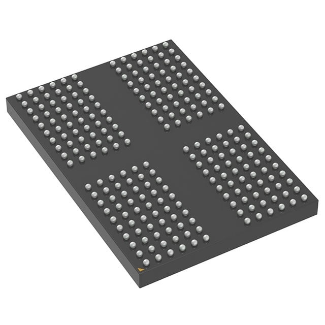
IC DRAM 32GBIT PAR 200TFBGA |
|---|---|
| Quantity | 551 Available (as of June 14, 2026) |

| Product Category | Memory |
|---|---|
| Manufacturer | Micron Technology Inc. |
| Manufacturing Status | Active |
| Manufacturer Standard Lead Time | 39 Weeks |
| Datasheet |
Specifications & Environmental
| Device Package | 200-TFBGA (10x14.5) | Memory Format | DRAM | Technology | SDRAM - Mobile LPDDR4 | ||
|---|---|---|---|---|---|---|---|
| Memory Size | 32 Gbit | Access Time | 3.5 ns | Grade | Industrial | ||
| Clock Frequency | 2.133 GHz | Voltage | 1.06V ~ 1.17V | Memory Type | Volatile | ||
| Operating Temperature | -25°C ~ 85°C (TC) | Write Cycle Time Word Page | 18 ns | Packaging | 200-TFBGA | ||
| Mounting Method | Volatile | Memory Interface | Parallel | Memory Organization | 1G x 32 | ||
| Moisture Sensitivity Level | 3 (168 Hours) | RoHS Compliance | ROHS Compliant | REACH Compliance | REACH Unaffected | ||
| Qualification | N/A | ECCN | EAR99 | HTS Code | 8542.32.0036 |
Overview of MT53E1G32D2FW-046 WT:B – IC DRAM 32GBIT PAR 200TFBGA
The MT53E1G32D2FW-046 WT:B is a 32 Gbit LPDDR4 mobile SDRAM device organized as 1G × 32 with a parallel memory interface. It implements a 16n prefetch DDR architecture and delivers high-bandwidth operation at a 2133 MHz clock rate (4266 Mb/s data rate per pin).
Designed for space-constrained, high-throughput memory subsystems, this device combines low-voltage operation, advanced refresh and power features, and a compact 200-ball TFBGA (10 mm × 14.5 mm × 1.1 mm) package for embedded and mobile memory implementations.
Key Features
- Memory Core & Architecture 32 Gbit LPDDR4 SDRAM organized as 1G × 32 with 16n prefetch DDR architecture and 8 internal banks per channel for concurrent operation.
- Performance 2133 MHz clock rate delivering a 4266 Mb/s data rate per pin and up to 8.5 GB/s per die (x16 channel) as specified in the datasheet.
- Timing Write cycle time (word page) of 18 ns and access time of 3.5 ns; programmable READ and WRITE latencies (RL/WL) and selectable burst lengths (BL = 16, 32).
- Low-Voltage Power Options Ultra-low-voltage core and I/O supplies with datasheet-specified rails: VDD1 = 1.70–1.95 V, VDD2 = 1.06–1.17 V (device specification lists 1.06–1.17 V), and VDDQ options of 0.57–0.65 V or 1.06–1.17 V.
- Power Management & Refresh Directed per-bank refresh, partial-array self refresh (PASR), on-chip temperature sensor for self-refresh control, and clock-stop capability to optimize power usage and refresh scheduling.
- Signal & I/O Features Single-data-rate CMD/ADR entry, bidirectional/differential data strobe per byte lane, and programmable output drive strength (DS).
- Package & Thermal 200-ball TFBGA (10 mm × 14.5 mm × 1.1 mm, Ø0.40 SMD) package (FW variant) with an operating temperature range of −25°C to +85°C (WT temperature grade).
- Standards & Compliance LPDDR4/LPDDR4X unified product family features and RoHS-compliant packaging as noted in the datasheet.
Typical Applications
- Mobile devices — LPDDR4 mobile SDRAM technology and low-voltage operation support implementation as system memory in mobile memory subsystems.
- Compact embedded systems — 32 Gbit capacity in a 200-TFBGA (10 mm × 14.5 mm) package suits designs with tight board-space constraints.
- High-bandwidth buffers and system memory — 1G × 32 organization, 16n prefetch, and 4266 Mb/s per-pin data rates enable use where sustained throughput is required.
Unique Advantages
- High per-pin data throughput: 4266 Mb/s data rate per pin at 2133 MHz clock supports demanding memory bandwidth needs.
- Low-voltage operation: Multiple VDD rails (VDD1, VDD2, VDDQ) including ultra-low-voltage options reduce core and I/O power envelope.
- Advanced refresh control: Directed per-bank refresh and partial-array self refresh allow finer refresh scheduling and improved concurrency.
- Compact FBGA package: 200-ball TFBGA (10 mm × 14.5 mm × 1.1 mm) provides high density in a small footprint for space-limited designs.
- On-die management features: On-chip temperature sensor, programmable RL/WL, and selectable drive strength enable adaptable performance and thermal management.
- Industry-standard LPDDR4 family: Part of Micron’s LPDDR4/LPDDR4X product set, enabling consistent architecture and specification alignment within the family.
Why Choose MT53E1G32D2FW-046 WT:B?
The MT53E1G32D2FW-046 WT:B positions itself as a high-density LPDDR4 memory die that delivers mobile-class bandwidth and low-voltage operation in a compact 200-ball TFBGA package. Its combination of 1G × 32 organization, 4266 Mb/s per-pin data rates, and on-die power/refresh features make it suitable for designs that require high throughput and careful power/thermal management.
This device is appropriate for engineers specifying LPDDR4-class memory where a 32 Gbit capacity, programmable timing, and space-efficient packaging are required. As part of Micron’s LPDDR4/LPDDR4X product family, it provides a defined feature set for integration into embedded and mobile memory subsystems.
Request a quote or submit an inquiry for pricing and availability of the MT53E1G32D2FW-046 WT:B to receive product lead-time and ordering information.