MT53E512M64D2HJ-046 WT:B
| Part Description |
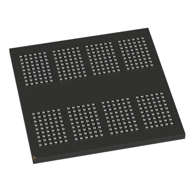
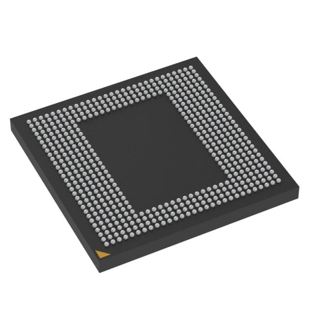
IC DRAM 32GBIT PAR 556WFBGA |
|---|---|
| Quantity | 1,372 Available (as of June 17, 2026) |

| Product Category | DRAM Memory |
|---|---|
| Manufacturer | Micron Technology Inc. |
| Manufacturing Status | Active |
| Manufacturer Standard Lead Time | 39 Weeks |
| Datasheet |
Specifications & Environmental
| Device Package | 556-WFBGA (12.4x12.4) | Memory Format | DRAM | Technology | SDRAM - Mobile LPDDR4 | ||
|---|---|---|---|---|---|---|---|
| Memory Size | 32 Gbit | Access Time | 3.5 ns | Grade | Industrial | ||
| Clock Frequency | 2.133 GHz | Voltage | 1.06V ~ 1.17V | Memory Type | Volatile | ||
| Operating Temperature | -25°C ~ 85°C (TC) | Write Cycle Time Word Page | 18 ns | Packaging | 556-TFBGA | ||
| Mounting Method | Volatile | Memory Interface | Parallel | Memory Organization | 512M x 64 | ||
| Moisture Sensitivity Level | N/A | RoHS Compliance | ROHS Compliant | REACH Compliance | REACH Unaffected | ||
| Qualification | N/A | ECCN | N/A | HTS Code | N/A |
Overview of MT53E512M64D2HJ-046 WT:B – IC DRAM 32GBIT PAR 556WFBGA
The MT53E512M64D2HJ-046 WT:B is a 32 Gbit volatile DRAM device implemented in a mobile LPDDR4/LPDDR4X SDRAM architecture. It uses a 512M x 64 memory organization with a parallel memory interface and is offered in a 556-ball W/TFBGA package (12.4 mm × 12.4 mm).
Designed for systems that require high-bandwidth, low-voltage DRAM, this device delivers 2133 MHz clock operation (4266 Mb/s data rate per pin) along with low-voltage supply options and features to support efficient power and refresh management.
Key Features
- Core and I/O voltages — Supports multiple supply rails: VDD1 = 1.70–1.95 V (core), VDD2 = 1.06–1.17 V, and selectable VDDQ = 0.57–0.65 V or 1.06–1.17 V.
- High-bandwidth operation — Clock rate 2133 MHz with a per-pin data rate of 4266 Mb/s; architecture supports 16n prefetch and programmable burst lengths (BL = 16, 32).
- Memory organization — 32 Gbit total capacity arranged as 512M × 64 (4 channels × 16 I/O) for parallel channel operation.
- Performance timing — Write cycle time (word page) 18 ns and access time 3.5 ns; speed grade -046 timing parameters defined for RL/WL and DBI options.
- Power and low-power modes — Ultra-low-voltage core and I/O supplies, clock-stop capability, and programmable output drive strength to optimize power vs. performance.
- Refresh and reliability features — Directed per-bank refresh for concurrent bank operation, partial-array self refresh (PASR), programmable VSS (ODT) termination, and an on-chip temperature sensor to control self-refresh rate.
- Package and thermal — 556-ball TFBGA package (12.4 mm × 12.4 mm, Ø0.24 SMD), operating temperature range −25°C to +85°C (WT option).
Typical Applications
- Mobile and handheld devices — Low-voltage operation and high per-pin data rate suit compact systems requiring high bandwidth and tight power budgets.
- Embedded memory subsystems — Parallel 512M × 64 organization and banked architecture support concurrent transactions in embedded compute modules.
- High-performance modules — Programmable latencies, burst lengths, and selectable drive strength enable tuning for module-level memory performance.
Unique Advantages
- Low-voltage operation: Multiple VDD options (including VDD2 = 1.06–1.17 V and VDDQ low-voltage option) reduce core and I/O power consumption where supported.
- High sustained bandwidth: 2133 MHz clock with 4266 Mb/s per-pin data rate and 16n prefetch for high-throughput memory channels.
- Fine-grain refresh control: Directed per-bank refresh and PASR enable concurrent bank operation and reduced refresh overhead for active regions of memory.
- Thermal-aware operation: On-chip temperature sensor can adjust self-refresh behavior to maintain reliability across the specified −25°C to +85°C range.
- Flexible I/O configuration: Selectable VDDQ and programmable output drive strength allow designers to match signaling levels and drive to system requirements.
Why Choose MT53E512M64D2HJ-046 WT:B?
This LPDDR4/LPDDR4X-based 32 Gbit DRAM provides a combination of high per-pin data rate, low-voltage operation, and advanced refresh/power management features that make it suitable for designs needing compact, high-bandwidth memory. Its 512M × 64 organization with 4 channels × 16 I/O supports parallel throughput and concurrent access patterns.
Engineers seeking a memory device that balances performance, configurable signaling, and thermal-aware refresh options will find this part useful for embedded, mobile, and module-level memory subsystems. The device’s package and specified operating range align with assemblies targeting commercial temperature environments.
If you require pricing, availability, or a formal quote for MT53E512M64D2HJ-046 WT:B, please request a quote or submit an inquiry to our sales team for further assistance.