MT53E512M64D2NW-046 IT:B
| Part Description |
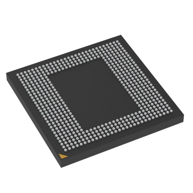
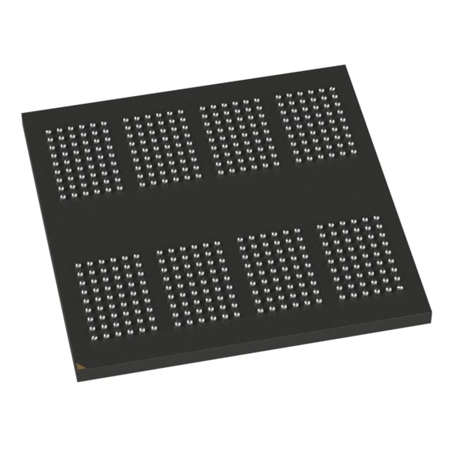
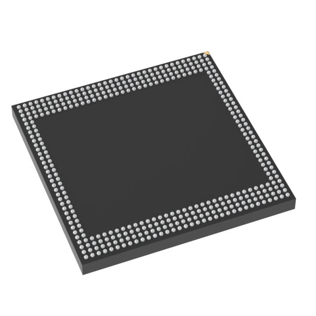
IC DRAM 32GBIT 432VFBGA |
|---|---|
| Quantity | 834 Available (as of June 18, 2026) |

| Product Category | DRAM Memory |
|---|---|
| Manufacturer | Micron Technology Inc. |
| Manufacturing Status | Active |
| Manufacturer Standard Lead Time | 26 Weeks |
| Datasheet |
Specifications & Environmental
| Device Package | 432-VFBGA (15x15) | Memory Format | DRAM | Technology | SDRAM - Mobile LPDDR4 | ||
|---|---|---|---|---|---|---|---|
| Memory Size | 32 Gbit | Access Time | N/A | Grade | N/A | ||
| Clock Frequency | N/A | Voltage | N/A | Memory Type | N/A | ||
| Operating Temperature | N/A | Write Cycle Time Word Page | N/A | Packaging | 432-VFBGA | ||
| Mounting Method | N/A | Memory Interface | N/A | Memory Organization | N/A | ||
| Moisture Sensitivity Level | 3 (168 Hours) | RoHS Compliance | ROHS3 Compliant | REACH Compliance | REACH Unaffected | ||
| Qualification | N/A | ECCN | N/A | HTS Code | N/A |
Overview of MT53E512M64D2NW-046 IT:B – IC DRAM 32GBIT 432VFBGA
The MT53E512M64D2NW-046 IT:B is a 32 Gbit LPDDR4X/LPDDR4 DRAM device in a 432‑VFBGA (15×15) package. It implements mobile LPDDR4 architecture and is supplied with a -046 speed grade that defines a 2133 MHz clock rate and a 4266 Mb/s data rate per pin.
Designed for applications that require mobile LPDDR4 class memory, the device combines multi‑channel SDRAM architecture, low‑voltage operation and package density to deliver bandwidth and integration suitable for space‑constrained, high‑performance modules.
Key Features
- Memory Architecture LPDDR4X/LPDDR4 SDRAM architecture with 16n prefetch and up to 8 internal banks per channel for concurrent operation.
- Performance Speed grade -046: clock rate 2133 MHz with a data rate per pin of 4266 Mb/s; supports programmable READ/WRITE latencies and burst lengths (BL = 16, 32).
- Power and Voltage Options Ultra‑low‑voltage core and I/O supplies. Documented supply ranges include VDD1 = 1.70–1.95 V (1.80 V nominal), VDD2 = 1.06–1.17 V (1.10 V nominal), and VDDQ options (0.57–0.65 V nominal 0.60 V or 1.06–1.17 V nominal 1.10 V).
- Throughput per Channel Up to 8.5 GB/s per die on a x16 channel (as specified in the device feature set).
- Refresh and Reliability Features Directed per‑bank refresh, partial‑array self refresh (PASR) and an on‑chip temperature sensor to control self refresh behavior.
- I/O and Signal Single‑data‑rate CMD/ADR entry, bidirectional/differential data strobe per byte lane, selectable output drive strength, and programmable ODT termination.
- Package 432‑VFBGA package (15×15 mm) for compact, high‑density board integration; marked with revision :B and special option suffixes as specified by part number.
- Environmental RoHS‑compliant, “green” packaging as noted in the product datasheet.
Typical Applications
- Mobile and Portable Systems — Memory for mobile LPDDR4 class devices where low voltage and compact package footprint are required.
- High‑Bandwith SoC Memory — Shared DRAM resource for system‑on‑chip designs that require multi‑bank concurrency and programmable latencies.
- Embedded Multimedia and Imaging — Frame buffer and data buffering applications that benefit from high per‑pin data rates and large capacity.
Unique Advantages
- High per‑pin data rate: The -046 speed grade provides 4266 Mb/s per pin (2133 MHz clock rate), enabling substantial bandwidth in designs that require fast memory access.
- Low‑voltage operation: Multiple documented VDD options (VDD1, VDD2, VDDQ) support ultra‑low power core and I/O operation for power‑sensitive designs.
- Compact, high‑density package: 432‑VFBGA (15×15) package delivers 32 Gbit density in a small board footprint for space‑constrained systems.
- Concurrent bank operation: Eight internal banks per channel and directed per‑bank refresh simplify command scheduling for sustained throughput.
- Die‑in‑package configuration: The D2 device configuration denotes two dies in package, as defined in the device ordering options.
- On‑chip management features: Built‑in temperature sensor and PASR support reduce external management overhead for refresh and power control.
Why Choose MT53E512M64D2NW-046 IT:B?
The MT53E512M64D2NW-046 IT:B positions itself as a 32 Gbit LPDDR4X/LPDDR4 memory building block combining mobile SDRAM architecture, documented low‑voltage supply options and a compact 432‑VFBGA footprint. Its -046 speed grade specification (2133 MHz / 4266 Mb/s per pin), multi‑bank architecture and on‑chip management features make it suitable for designs that need high throughput, scalable capacity and tight board integration.
This device is appropriate for engineers and procurement teams specifying LPDDR4‑class memory for mobile, embedded multimedia and SoC memory subsystems that require verifiable electrical and timing characteristics as provided in the device datasheet.
Request a quote or submit a procurement inquiry for MT53E512M64D2NW-046 IT:B to obtain current availability and pricing information.