MT53E512M64D2NZ-46 WT:B TR
| Part Description |
IC DRAM 32GBIT PAR 376WFBGA |
|---|---|
| Quantity | 1,165 Available (as of June 15, 2026) |
| Product Category | DRAM Memory |
|---|---|
| Manufacturer | Micron Technology Inc. |
| Manufacturing Status | Active |
| Manufacturer Standard Lead Time | 6 Weeks |
| Datasheet |
Specifications & Environmental
| Device Package | 376-WFBGA (14x14) | Memory Format | DRAM | Technology | SDRAM - Mobile LPDDR4 | ||
|---|---|---|---|---|---|---|---|
| Memory Size | 32 Gbit | Access Time | 3.5 ns | Grade | Industrial | ||
| Clock Frequency | 2.133 GHz | Voltage | 1.06V ~ 1.17V | Memory Type | Volatile | ||
| Operating Temperature | -25°C ~ 85°C (TC) | Write Cycle Time Word Page | 18 ns | Packaging | 376-WFBGA | ||
| Mounting Method | Volatile | Memory Interface | Parallel | Memory Organization | 512M x 64 | ||
| Moisture Sensitivity Level | N/A | RoHS Compliance | ROHS3 Compliant | REACH Compliance | REACH Unaffected | ||
| Qualification | N/A | ECCN | N/A | HTS Code | N/A |
Overview of MT53E512M64D2NZ-46 WT:B TR – IC DRAM 32GBIT PAR 376WFBGA
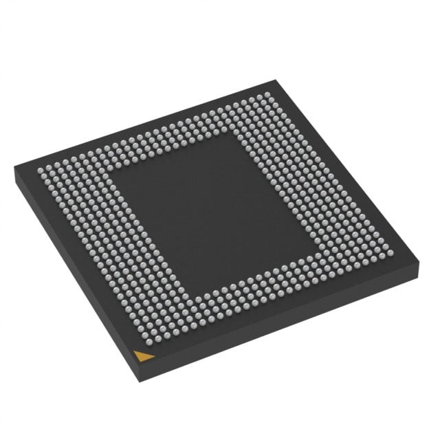
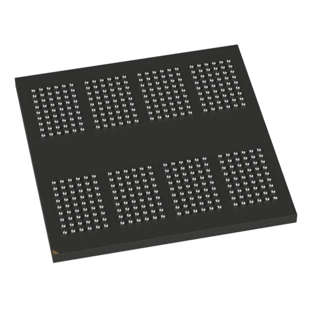
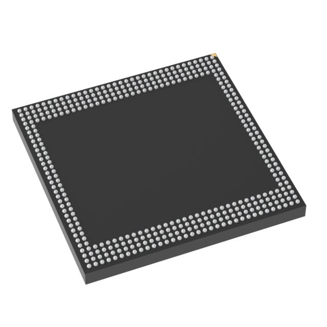
The MT53E512M64D2NZ-46 WT:B TR is a 32 Gbit volatile DRAM device based on Mobile LPDDR4/LPDDR4X SDRAM architecture. It is organized as 512M x 64 with a parallel memory interface and is offered in a 376-ball WFBGA (14 × 14 mm) package.
Designed for high-bandwidth embedded memory applications, the part provides low-voltage operation and programmable timing options to support systems requiring fast access, high data rates, and compact BGA packaging.
Key Features
- Memory Core and Architecture 32 Gbit DRAM organized as 512M x 64 with 16n prefetch DDR architecture and up to 8 internal banks per channel for concurrent operation.
- Technology Mobile LPDDR4/LPDDR4X SDRAM technology with support for programmable READ and WRITE latencies and on-the-fly burst length selection (BL = 16, 32).
- Performance Clock rate 2133 MHz (2.133 GHz) with a data rate per pin of 4266 Mb/s and an access time of 3.5 ns. Write cycle time (word page) is 18 ns.
- Power Supply Options Supports ultra-low-voltage supplies including VDD1 = 1.70–1.95 V, VDD2 = 1.06–1.17 V (listed in product specs as 1.06–1.17 V), and VDDQ options 0.57–0.65 V or 1.06–1.17 V depending on configuration.
- Power and Low-Power Features On-chip temperature sensor for self-refresh control, partial-array self refresh (PASR), programmable VSS (ODT) termination, and clock-stop capability to reduce power in idle states.
- Command and I/O Single-data-rate CMD/ADR entry, bidirectional/differential data strobe per byte lane, selectable output drive strength, and support for single-ended CK and DQS.
- Package and Mounting 376-WFBGA (14 × 14 mm, 0.71 mm height) supplier device package; surface-mount BGA package suitable for compact system designs.
- Operating Range Temperature grade TC: –25°C to +85°C (operating temperature).
- Reliability and Manufacturing FBGA “green” packaging and programmable directed per-bank refresh for concurrent bank operation and simplified command scheduling.
Typical Applications
- Mobile and Handheld Devices High-bandwidth embedded memory for compact systems that require LPDDR4/LPDDR4X low-voltage operation and BGA packaging.
- Consumer Electronics Memory subsystem for devices needing fast random access and configurable burst lengths to match varying workload patterns.
- Embedded Systems On-board parallel DRAM for designs that benefit from multiple internal banks, directed per-bank refresh, and programmable latencies.
Unique Advantages
- High data rate capability: 2133 MHz clock with 4266 Mb/s per pin supports demanding throughput requirements.
- Flexible timing and bursts: Programmable READ/WRITE latencies and selectable burst lengths (BL = 16, 32) enable tuning for different system behaviors.
- Low-voltage operation: Multiple core and I/O supply options (including VDD2 = 1.06–1.17 V and VDDQ low-voltage options) reduce power draw in mobile contexts.
- Advanced refresh and thermal management: Directed per-bank refresh and an on-chip temperature sensor help maintain performance and power efficiency across workloads.
- Compact BGA package: 376-ball WFBGA (14 × 14 mm) offers high-density mounting for space-constrained PCBs.
- Concurrent bank operation: Eight internal banks per channel and 16n prefetch architecture support high concurrency and improved command scheduling.
Why Choose IC DRAM 32GBIT PAR 376WFBGA?
The MT53E512M64D2NZ-46 WT:B TR combines LPDDR4/LPDDR4X architecture, multi-gigahertz clocking, and low-voltage supply options to deliver a compact, high-throughput DRAM solution for embedded and mobile systems. Its programmable timing, advanced refresh features, and on-chip temperature monitoring provide design flexibility for performance and power trade-offs.
This device is well suited for engineers specifying high-density parallel DRAM in space-constrained designs who require clear electrical and thermal operating parameters and configurable memory timing. Its package and electrical options support integration into systems demanding both bandwidth and compact footprint.
If you would like pricing, availability, or to request a quotation for MT53E512M64D2NZ-46 WT:B TR, submit a sourcing inquiry or request a quote to evaluate this memory device for your design needs.