MT53E512M64D4HJ-046 AAT:D TR
| Part Description |
IC DRAM 32GBIT PAR 556WFBGA |
|---|---|
| Quantity | 61 Available (as of June 17, 2026) |

| Product Category | DRAM Memory |
|---|---|
| Manufacturer | Micron Technology Inc. |
| Manufacturing Status | Obsolete |
| Manufacturer Standard Lead Time | Contact Us |
| Datasheet |
Specifications & Environmental
| Device Package | 556-WFBGA (12.4x12.4) | Memory Format | DRAM | Technology | SDRAM - Mobile LPDDR4 | ||
|---|---|---|---|---|---|---|---|
| Memory Size | 32 Gbit | Access Time | N/A | Grade | N/A | ||
| Clock Frequency | N/A | Voltage | N/A | Memory Type | N/A | ||
| Operating Temperature | N/A | Write Cycle Time Word Page | N/A | Packaging | 556-TFBGA | ||
| Mounting Method | N/A | Memory Interface | Parallel | Memory Organization | 512M x 64 | ||
| Moisture Sensitivity Level | N/A | RoHS Compliance | N/A | REACH Compliance | REACH Unaffected | ||
| Qualification | N/A | ECCN | N/A | HTS Code | N/A |
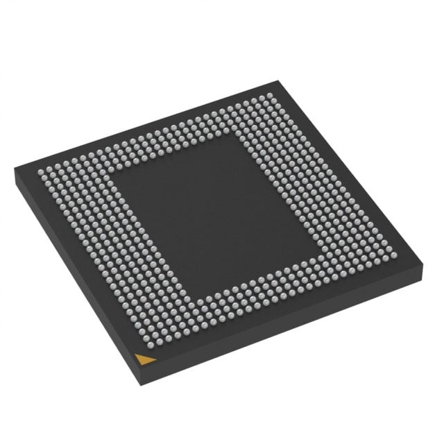
Overview of MT53E512M64D4HJ-046 AAT:D TR – IC DRAM 32GBIT PAR 556WFBGA
The MT53E512M64D4HJ-046 AAT:D TR is a 32 Gbit DRAM device implemented in Mobile LPDDR4/LPDDR4X SDRAM technology. It uses a parallel memory interface with a 512M x 64 organization and is supplied in a 556-ball WFBGA package (12.4 × 12.4 mm).
This device targets designs that require high-density, high-bandwidth mobile LPDDR4 memory with low-voltage supply options and integrated device-level features for memory management and power efficiency.
Key Features
- Technology / Architecture Mobile LPDDR4/LPDDR4X SDRAM architecture with 16n prefetch and 8 internal banks per channel for concurrent operation.
- Memory Organization & Capacity 512M × 64 organization delivering 32 Gbit total memory capacity in a multi-die package option.
- Performance Speed grade -046 supports a 2133 MHz clock rate and 4266 Mb/s data rate per pin (data rate per pin shown in datasheet).
- Low-Voltage Supply Options Datasheet lists nominal supply ranges including VDD1 = 1.70–1.95 V (1.80 V nominal), VDD2 = 1.06–1.17 V (1.10 V nominal), and VDDQ options of 0.57–0.65 V (0.60 V nominal) or 1.06–1.17 V (1.10 V nominal).
- Latency & Burst Control Programmable READ and WRITE latencies (RL/WL) and selectable burst lengths (BL = 16, 32) to tune performance for system requirements.
- Refresh & Reliability Features Directed per-bank refresh for concurrent bank operation, partial-array self refresh (PASR), and an on-chip temperature sensor to manage self-refresh behavior.
- I/O & Termination Bidirectional/differential data strobe per byte lane, selectable output drive strength (DS), programmable VSS (ODT) termination, and single-data-rate CMD/ADR entry.
- Package 556-ball TFBGA/WFBGA package option (12.4 × 12.4 mm) suitable for high-density mounting; package marking option HJ corresponds to this 556-ball package.
- Additional System Features Support for clock-stop capability and single-ended CK and DQS support as documented in the datasheet.
Typical Applications
- Mobile devices Mobile LPDDR4/LPDDR4X architecture is intended for handheld and mobile memory subsystems that require high density and low-voltage operation.
- High-bandwidth memory subsystems High per-pin data rate (4266 Mb/s) and multi-bank architecture support bandwidth-intensive tasks such as multimedia and graphics buffering.
- Low-voltage embedded designs Multiple low-voltage supply options and power-management features make it suitable for embedded systems that prioritize power efficiency.
Unique Advantages
- High-density in a compact package: 32 Gbit memory capacity implemented in a 556-ball WFBGA (12.4 × 12.4 mm) package for space-constrained systems.
- High per-pin throughput: Speed grade -046 provides a 2133 MHz clock and 4266 Mb/s per-pin data rate to meet demanding bandwidth requirements.
- Flexible voltage options: Multiple VDD1/VDD2/VDDQ ranges documented for LPDDR4X/LPDDR4 to match system power domains and efficiency targets.
- Software-tunable performance: Programmable RL/WL and burst-length options allow system designers to optimize latency and throughput trade-offs.
- System-level power management: Directed per-bank refresh, PASR and an on-chip temperature sensor help reduce active and standby power while maintaining data integrity.
- Integrated I/O control: Selectable output drive strength and programmable ODT provide signal integrity and termination flexibility for high-speed interfaces.
Why Choose IC DRAM 32GBIT PAR 556WFBGA?
The MT53E512M64D4HJ-046 AAT:D TR combines high density, mobile LPDDR4/LPDDR4X architecture and high per-pin data rates in a compact 556-ball WFBGA package, making it well suited for designs that require substantial memory capacity and bandwidth within a small footprint. Its programmable latency, burst control and power-management features allow designers to tune performance and power consumption to application needs.
This Micron DRAM device is appropriate for customers building mobile and embedded systems that require low-voltage operation, high throughput and integrated device-level features for refresh and thermal management. The documented voltage ranges, speed grade and package information support informed system integration and long-term design planning.
Request a quote or submit a product inquiry to confirm availability, lead times and pricing for this MT53E512M64D4HJ-046 AAT:D TR memory device.