NAND128W3A2BNXE
| Part Description |
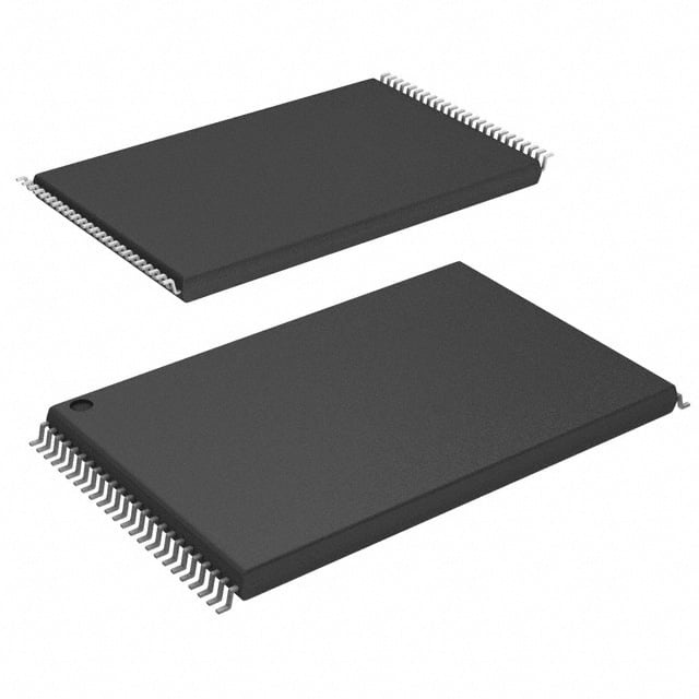
IC FLASH 128MBIT PAR 48TSOP I |
|---|---|
| Quantity | 267 Available (as of June 14, 2026) |

| Product Category | Memory |
|---|---|
| Manufacturer | Micron Technology Inc. |
| Manufacturing Status | Obsolete |
| Manufacturer Standard Lead Time | Contact Us |
| Datasheet |
Specifications & Environmental
| Device Package | 48-TSOP I | Memory Format | FLASH | Technology | FLASH - NAND | ||
|---|---|---|---|---|---|---|---|
| Memory Size | 128 Mbit | Access Time | 50 ns | Grade | Industrial | ||
| Clock Frequency | N/A | Voltage | 2.7V ~ 3.6V | Memory Type | Non-Volatile | ||
| Operating Temperature | -40°C ~ 85°C (TA) | Write Cycle Time Word Page | 50 ns | Packaging | 48-TFSOP (0.724", 18.40mm Width) | ||
| Mounting Method | Non-Volatile | Memory Interface | Parallel | Memory Organization | 16M x 8 | ||
| Moisture Sensitivity Level | 3 (168 Hours) | RoHS Compliance | ROHS3 Compliant | REACH Compliance | REACH Unaffected | ||
| Qualification | N/A | ECCN | 3A991B1A | HTS Code | 8542.32.0071 |
Overview of NAND128W3A2BNXE – IC FLASH 128Mbit PAR 48TSOP I
The NAND128W3A2BNXE is a 128 Mbit non-volatile FLASH NAND memory organized as 16M × 8 with a parallel interface. It delivers 50 ns access and write-cycle timing and operates from a 2.7 V to 3.6 V supply, packaged in a 48‑TSOP I (48‑TFSOP, 18.40 mm width) form factor.
This device is intended for applications requiring straightforward parallel NAND flash storage with defined performance and industrial temperature range support from −40°C to 85°C.
Key Features
- Memory Type & Technology Non-volatile FLASH — NAND architecture providing 128 Mbit storage organized as 16M × 8.
- Performance 50 ns access time and 50 ns write cycle time (word/page) for predictable read/write timing.
- Interface Parallel memory interface for direct integration with parallel host controllers and address/data bus designs.
- Power Single-supply operation from 2.7 V to 3.6 V to match common system voltage rails.
- Package 48‑TSOP I (48‑TFSOP, 0.724", 18.40 mm width) surface-mount package for compact PCB footprint.
- Operating Temperature −40°C to 85°C ambient range suitable for extended-temperature electronics applications.
Typical Applications
- Embedded non-volatile storage Provides 128 Mbit NAND FLASH storage in systems that require parallel memory access and compact TSOP packaging.
- Firmware and code storage Used where dedicated parallel FLASH storage with 16M × 8 organization and 50 ns timing is required for system boot or firmware images.
- Data buffering and logging Suitable for designs needing reliable non-volatile page/word write timing at standard 2.7 V–3.6 V supply levels.
Unique Advantages
- Defined timing performance: 50 ns access and write-cycle time enable predictable read/write behavior for timing-sensitive designs.
- Standard voltage compatibility: 2.7 V–3.6 V range aligns with common system rails, simplifying power-supply requirements.
- Compact TSOP packaging: 48‑TSOP I package (18.40 mm width) reduces PCB area while providing a standard surface-mount footprint.
- Industry temperature support: −40°C to 85°C operating range supports extended-temperature applications without additional thermal qualification notes.
- Parallel interface simplicity: Parallel memory interface enables direct connection to parallel buses and controllers, reducing interface complexity.
Why Choose NAND128W3A2BNXE?
NAND128W3A2BNXE offers a concise combination of 128 Mbit NAND FLASH capacity, 50 ns read/write timing, and a parallel interface in a 48‑TSOP I package. Its 2.7 V–3.6 V supply range and −40°C to 85°C operating window make it suitable for designs that need reliable non-volatile storage with defined electrical and thermal characteristics.
This device is appropriate for engineers integrating compact parallel FLASH memory where deterministic timing, standard supply compatibility, and a small surface-mount package are required.
Request a quote or submit a pricing inquiry for NAND128W3A2BNXE to check availability and discuss ordering options.