
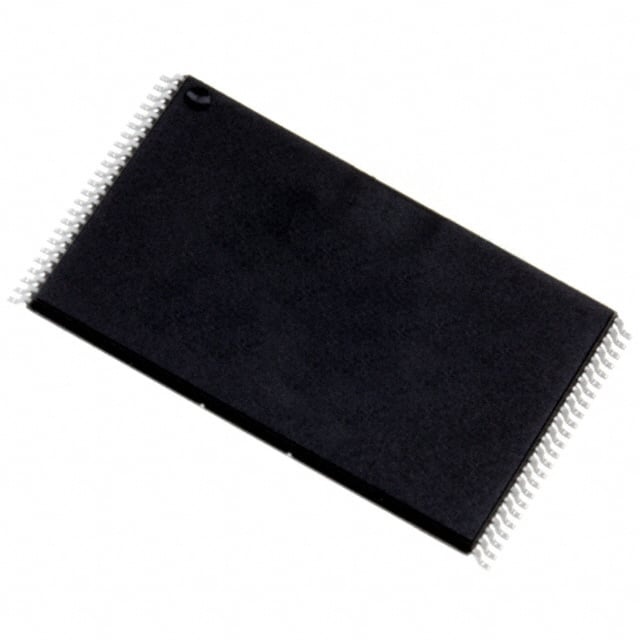
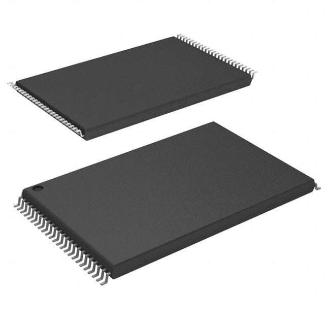
NAND256W4A0AN6E
| Part Description |
IC FLASH 256MBIT PARALLEL 48TSOP |
|---|---|
| Quantity | 757 Available (as of June 18, 2026) |
| Product Category | Flash Memory |
|---|---|
| Manufacturer | STMicroelectronics |
| Manufacturing Status | Obsolete |
| Manufacturer Standard Lead Time | Contact Us |
| Datasheet |
Specifications & Environmental
| Device Package | 48-TSOP | Memory Format | FLASH | Technology | FLASH - NAND | ||
|---|---|---|---|---|---|---|---|
| Memory Size | 256 Mbit | Access Time | 50 ns | Grade | Industrial | ||
| Clock Frequency | N/A | Voltage | 2.7V ~ 3.6V | Memory Type | Non-Volatile | ||
| Operating Temperature | -40°C ~ 85°C (TA) | Write Cycle Time Word Page | 50 ns | Packaging | 48-TFSOP (0.724", 18.40mm Width) | ||
| Mounting Method | Non-Volatile | Memory Interface | Parallel | Memory Organization | 16M x 16 | ||
| Moisture Sensitivity Level | 1 (Unlimited) | RoHS Compliance | ROHS3 Compliant | REACH Compliance | REACH Unaffected | ||
| Qualification | N/A | ECCN | 3A991B1A | HTS Code | 8542.32.0071 |
Overview of NAND256W4A0AN6E – IC FLASH 256Mbit Parallel 48‑TSOP
The NAND256W4A0AN6E is a 256 Mbit non-volatile NAND flash memory organized as 16M × 16 with a parallel (x16) interface in a 48‑TSOP footprint. It targets mass-storage and embedded boot applications that require parallel NAND architecture, 3.0 V supply operation, and commercial temperature operation.
Built on NAND flash technology, the device offers block erase and page program/read operations, on‑chip data protection features and development support items documented in the product datasheet.
Key Features
- Memory Architecture — 256 Mbit NAND flash organized as 16M × 16 (x16 bus width) with page and block structure suitable for mass storage implementations.
- Interface — Parallel NAND interface (x16) with multiplexed address/data signals and pinout compatibility across densities.
- Performance — Sequential access timing down to 50 ns (min); random page access up to 12 μs (max); typical page program time ~200 μs and typical block erase time ~2 ms as documented.
- Supply and Timing — 3.0 V device operating range VDD = 2.7 V to 3.6 V; write/read timing including 50 ns word/page write-cycle timing available.
- Endurance and Retention — Documented for 100,000 program/erase cycles and 10 years data retention in the datasheet.
- Data Protection & Reliability — Hardware data protection during power transitions, status register and electronic signature features, and built‑in bad block management concepts described in the datasheet.
- Advanced Flash Functions — Supports copy‑back program mode (fast page copy without external buffering) and optional automatic page 0 read at power‑up for boot support.
- Package & Temperature — Supplied in a 48‑TSOP package (0.724" / 18.40 mm width) and specified for operation from −40 °C to +85 °C (TA).
- Development Resources — Documentation references ECC software/hardware models, bad block management and wear leveling algorithms, and PC demo boards for development and evaluation.
Typical Applications
- Mass storage solutions — Use in cost‑effective NAND flash storage arrays where a parallel x16 interface and block/page management are required.
- Embedded boot and firmware storage — Automatic page‑0 read at power‑up and boot support options enable system boot and automatic memory download workflows.
- Development and evaluation — Designed for use with provided demo boards, ECC models and reference software for firmware and file‑system development.
Unique Advantages
- Parallel x16 organization: Enables 16‑bit data transfers for systems designed around parallel NAND interfaces, matching legacy and embedded controller requirements.
- Wide VDD operating range: 2.7 V to 3.6 V support simplifies integration into 3.0 V systems.
- Documented endurance and retention: 100,000 program/erase cycles and 10 years data retention provide predictable lifecycle planning for storage applications.
- Fast internal operations: Sequential access to 50 ns (min), page program ~200 μs (typ) and block erase ~2 ms (typ) support responsive read/program/erase sequences.
- On‑chip functional support: Copy‑back program mode, status register and electronic signature options reduce external buffering and simplify firmware handling of flash operations.
- Development support ecosystem: Provided ECC models, bad block management and demo board references accelerate integration and validation activities.
Why Choose NAND256W4A0AN6E?
The NAND256W4A0AN6E from STMicroelectronics is positioned for designs that require a 256 Mbit parallel NAND flash with a 16‑bit data bus, documented performance characteristics, and practical endurance and retention figures. Its supply voltage range, package options and on‑chip flash functions make it suitable for embedded systems and mass storage applications that rely on predictable NAND behavior.
With development resources referenced in the datasheet—ECC/hardware models, bad block management guidance and demo board support—this device is aimed at engineers and procurement teams focusing on reliable integration, firmware development and long‑term data retention planning.
Request a quote or submit a purchase inquiry through your preferred distributor or sales channel to obtain pricing and availability for NAND256W4A0AN6E.


Date Founded: 1987
Headquarters: Plan-les-Ouates, Geneva, Switzerland
Employees: 50,000+
Revenue: $17.24 Billion
Certifications and Memberships: ISO9001:2015, ISO14001:2015, ISO45001:2018, IATF16949:2016, ISO50001:2018


