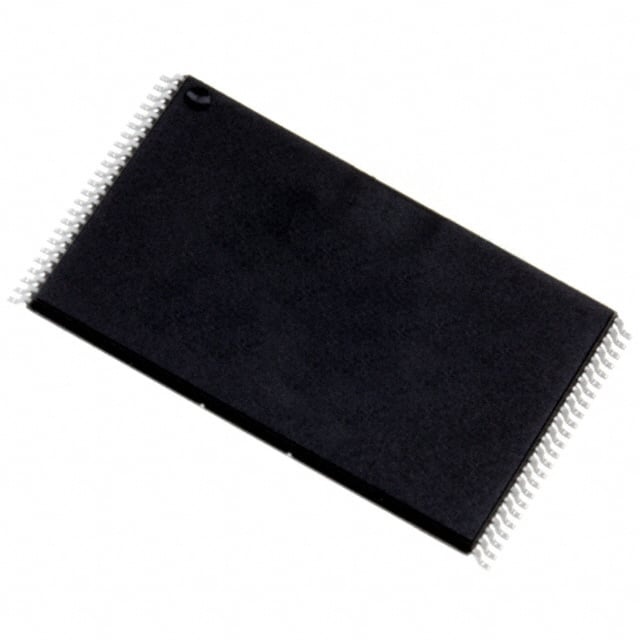
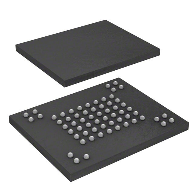
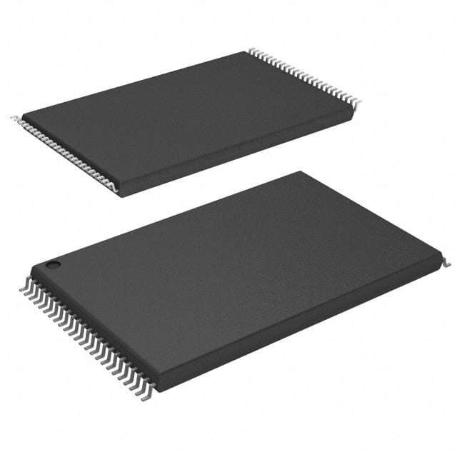
NAND32GW3F4AN6E
| Part Description |
IC FLASH 32GBIT PARALLEL 48TSOP |
|---|---|
| Quantity | 180 Available (as of June 9, 2026) |
| Product Category | Memory |
|---|---|
| Manufacturer | Micron Technology Inc. |
| Manufacturing Status | Obsolete |
| Manufacturer Standard Lead Time | Contact Us |
| Datasheet |
Specifications & Environmental
| Device Package | 48-TSOP | Memory Format | FLASH | Technology | FLASH - NAND | ||
|---|---|---|---|---|---|---|---|
| Memory Size | 32 Gbit | Access Time | 50 ns | Grade | Industrial | ||
| Clock Frequency | N/A | Voltage | 2.7V ~ 3.6V | Memory Type | Non-Volatile | ||
| Operating Temperature | -40°C ~ 85°C (TA) | Write Cycle Time Word Page | 50 ns | Packaging | 48-TFSOP (0.724", 18.40mm Width) | ||
| Mounting Method | Non-Volatile | Memory Interface | Parallel | Memory Organization | 4G x 8 | ||
| Moisture Sensitivity Level | 3 (168 Hours) | RoHS Compliance | ROHS3 Compliant | REACH Compliance | REACH Unaffected | ||
| Qualification | N/A | ECCN | 3A991B1A | HTS Code | 8542.32.0051 |
Overview of NAND32GW3F4AN6E – IC FLASH 32GBIT PARALLEL 48TSOP
The NAND32GW3F4AN6E is a 32‑Gbit SLC NAND flash memory device organized as 4 × 8 Gbit dice and presented with a parallel x8 interface. The device implements a multiplane architecture with two Chip Enable pins, allowing the array to be accessed as two independent 16‑Gbit devices.
Designed for mass storage and embedded storage applications, the device delivers large non‑volatile capacity in a 48‑lead TSOP package with a 2.7 V to 3.6 V supply range and an extended operating temperature range of −40 °C to 85 °C.
Key Features
- Core / Memory Architecture 32 Gbit SLC NAND organized as 4 × 8 Gbit dice with two Chip Enable signals; array split into two independent planes for parallel operation.
- Page & Block Organization Page size of 4,096 bytes + 128‑byte spare (4,224 bytes total); block size of 256 Kbytes + 8 Kbytes spare.
- Interface Parallel NAND interface with an x8 data bus width and multiplexed address/data pins.
- Performance Access timing referenced at 50 ns; datasheet timing notes sequential access 25 ns (min) and random access up to 25 μs (max). Typical page program time is 500 μs and typical block erase time is 1.5 ms.
- Power Single‑supply operation over VDD = 2.7 V to 3.6 V.
- Reliability & Data Integrity Specified for 100,000 program/erase cycles (with ECC) and 10 years data retention; includes status register, electronic signature, and OTP area and unique serial number for device identification.
- Advanced NAND Features Multiplane operation with the ability to perform operations on both planes simultaneously, copy‑back program, automatic block download without latency, and multiblock erase.
- Package & Temperature 48‑lead TSOP package (48‑TFSOP / 48‑TSOP noted; package mechanical details in datasheet) and operating temperature range −40 °C to 85 °C.
Typical Applications
- Mass Storage Solutions High‑density SLC NAND provides cost‑effective non‑volatile storage for mass storage applications.
- Embedded Storage Parallel x8 interface and large page/block organization for embedded systems requiring block‑oriented flash storage.
- Systems Requiring Wide Temperature Operation Operation from −40 °C to 85 °C supports use in environments with extended temperature ranges.
Unique Advantages
- High‑density SLC Capacity: 32 Gbit array (4 × 8 Gbit) provides substantial non‑volatile storage in a single device to reduce BOM count.
- Independent Dual Access: Two Chip Enable pins and plane split enable independent access to two 16‑Gbit domains for flexible system partitioning and parallel operations.
- Full NAND Feature Set: Support for copy‑back program, multiblock erase, status register, and electronic signature simplifies advanced flash management.
- Robust Endurance & Retention: Specified 100,000 program/erase cycles with ECC and 10 years data retention address long‑life storage needs.
- Flexible Power & Timing: Broad supply range (2.7 V–3.6 V) and documented access and program/erase timings allow integration into a variety of system designs.
- Package Options for Board Integration: 48‑lead TSOP package formats provided to suit common board‑level assembly and footprint requirements.
Why Choose NAND32GW3F4AN6E?
The NAND32GW3F4AN6E positions itself as a high‑density, SLC NAND flash device that combines large capacity, independent dual‑plane access, and a parallel x8 interface for systems requiring block‑oriented non‑volatile storage. Its documented program/erase timings, endurance specification with ECC, and long data retention make it suitable for storage‑focused embedded designs that need predictable flash behavior.
Engineers selecting this device gain a combination of capacity, standard parallel NAND interfacing, and feature support (copy‑back, multiblock erase, OTP, unique ID) that simplify flash management and system partitioning while operating across a wide voltage and temperature range.
Request a quote or contact sales to discuss availability, lead times, and volume pricing for the NAND32GW3F4AN6E.