NAND512R3A2DZA6E
| Part Description |
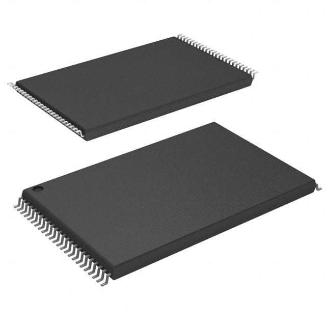
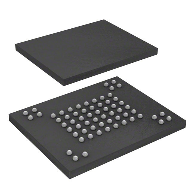
IC FLASH 512MBIT PAR 63VFBGA |
|---|---|
| Quantity | 62 Available (as of June 15, 2026) |
| Product Category | Memory |
|---|---|
| Manufacturer | Micron Technology Inc. |
| Manufacturing Status | Obsolete |
| Manufacturer Standard Lead Time | Contact Us |
| Datasheet |
Specifications & Environmental
| Device Package | 63-VFBGA (9x11) | Memory Format | FLASH | Technology | FLASH - NAND | ||
|---|---|---|---|---|---|---|---|
| Memory Size | 512 Mbit | Access Time | 50 ns | Grade | Industrial | ||
| Clock Frequency | N/A | Voltage | 1.7V ~ 1.95V | Memory Type | Non-Volatile | ||
| Operating Temperature | -40°C ~ 85°C (TA) | Write Cycle Time Word Page | 50 ns | Packaging | 63-TFBGA | ||
| Mounting Method | Non-Volatile | Memory Interface | Parallel | Memory Organization | 64M x 8 | ||
| Moisture Sensitivity Level | 3 (168 Hours) | RoHS Compliance | ROHS3 Compliant | REACH Compliance | REACH Unaffected | ||
| Qualification | N/A | ECCN | 3A991B1A | HTS Code | 8542.32.0071 |
Overview of NAND512R3A2DZA6E – IC FLASH 512MBIT PAR 63VFBGA
The NAND512R3A2DZA6E is a 512 Mbit non-volatile FLASH memory device using NAND technology with a parallel interface. It is organized as 64M × 8 and delivers defined access and write timings for embedded storage applications.
The device is supplied in a 63-VFBGA (9×11) package and operates from a 1.7 V to 1.95 V supply rail with an approved ambient operating range of −40°C to 85°C.
Key Features
- Memory
512 Mbit capacity implemented as 64M × 8; NAND flash non-volatile storage. - Performance
Access time of 50 ns and a write cycle time (word/page) of 50 ns for deterministic read/write timing. - Interface
Parallel memory interface organized as an 8-bit data bus for direct connection to parallel controllers. - Power
Nominal operating supply range of 1.7 V to 1.95 V. - Package
63-TFBGA package, supplied as 63-VFBGA (9×11) footprint for compact board-level integration. - Temperature Range
Rated for operation from −40°C to 85°C (TA).
Unique Advantages
- High-density storage in a compact footprint: 512 Mbit capacity in a 63-VFBGA (9×11) package enables significant on-board non-volatile storage while conserving PCB area.
- Deterministic timing: 50 ns access and 50 ns write cycle times provide predictable read/write behavior for system timing analysis.
- Parallel interface simplicity: 8-bit parallel organization supports direct interfacing to parallel memory controllers and legacy parallel systems.
- Low-voltage operation: 1.7 V to 1.95 V supply range supports designs targeting lower supply rails.
- Extended ambient temperature support: −40°C to 85°C operating range accommodates applications exposed to wide temperature conditions.
Why Choose NAND512R3A2DZA6E?
NAND512R3A2DZA6E is positioned for designs that require a mid-density NAND flash device with defined access and write timings, a parallel interface, and low-voltage operation. Its 63-VFBGA (9×11) package delivers a compact form factor for systems where board space is constrained.
This device is suited to customers specifying a 512 Mbit parallel NAND FLASH with clear electrical and thermal parameters, offering predictable integration into systems that require specified timing, supply, and temperature characteristics.
Request a quote or submit an inquiry for pricing and availability of NAND512R3A2DZA6E. Provide your quantity and lead-time requirements to receive a tailored response.