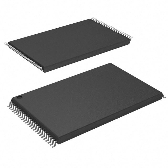
NAND512R3A2SN6F
| Part Description |
IC FLASH 512MBIT PAR 48TSOP I |
|---|---|
| Quantity | 420 Available (as of June 15, 2026) |
| Product Category | Memory |
|---|---|
| Manufacturer | Micron Technology Inc. |
| Manufacturing Status | Obsolete |
| Manufacturer Standard Lead Time | Contact Us |
| Datasheet |
Specifications & Environmental
| Device Package | 48-TSOP I | Memory Format | FLASH | Technology | FLASH - NAND | ||
|---|---|---|---|---|---|---|---|
| Memory Size | 512 Mbit | Access Time | 50 ns | Grade | Industrial | ||
| Clock Frequency | N/A | Voltage | 1.7V ~ 1.95V | Memory Type | Non-Volatile | ||
| Operating Temperature | -40°C ~ 85°C (TA) | Write Cycle Time Word Page | 50 ns | Packaging | 48-TFSOP (0.724", 18.40mm Width) | ||
| Mounting Method | Non-Volatile | Memory Interface | Parallel | Memory Organization | 64M x 8 | ||
| Moisture Sensitivity Level | 3 (168 Hours) | RoHS Compliance | ROHS3 Compliant | REACH Compliance | REACH Unknown | ||
| Qualification | N/A | ECCN | 3A991B1A | HTS Code | 8542.32.0071 |
Overview of NAND512R3A2SN6F – IC FLASH 512MBIT PAR 48TSOP I
The NAND512R3A2SN6F is a 512 Mbit non-volatile NAND flash memory device organized as 64M × 8 with a parallel memory interface. It delivers 50 ns access and 50 ns word/page write cycle times in a 48-TSOP I package while operating from a 1.7 V to 1.95 V supply and an ambient temperature range of −40°C to 85°C.
This device is intended for systems requiring parallel NAND flash storage with defined timing, low-voltage operation, and a compact TSOP footprint.
Key Features
- Memory — 512 Mbit capacity, organized as 64M × 8 in non-volatile FLASH (NAND) technology.
- Interface — Parallel memory interface for parallel data transfers.
- Performance — 50 ns access time and 50 ns write cycle time (word/page) to support rapid read/write operations.
- Power — Operates from a 1.7 V to 1.95 V supply voltage.
- Package — 48-TFSOP / 48-TSOP I package (0.724", 18.40 mm width) for a compact PCB footprint.
- Temperature Range — Rated for operation from −40°C to 85°C (TA).
- Technology — FLASH - NAND memory format.
Unique Advantages
- High-density storage: 512 Mbit in a single device (64M × 8) provides substantial non-volatile capacity without multiple components.
- Predictable timing: 50 ns access and write cycle times enable deterministic read/write performance.
- Low-voltage operation: 1.7 V to 1.95 V supply range supports lower-voltage system designs.
- Compact TSOP footprint: 48-TSOP I package (0.724", 18.40 mm width) conserves PCB space while providing parallel pinout.
- Broad thermal tolerance: −40°C to 85°C operating range accommodates a wide ambient temperature envelope.
Why Choose NAND512R3A2SN6F?
The NAND512R3A2SN6F from Micron Technology Inc. combines 512 Mbit parallel NAND architecture with 50 ns access and write timings in a compact 48-TSOP I package, and operates on a low 1.7 V–1.95 V supply across −40°C to 85°C. These characteristics make it a practical choice when capacity, defined timing, package footprint, and low-voltage operation are primary selection criteria.
This part is suitable for engineers and procurement teams specifying parallel NAND flash memory where a single-component, high-density, low-voltage solution is required.
Request a quote or submit a pricing and availability inquiry for NAND512R3A2SN6F to receive lead time and ordering information through your preferred procurement channel.